Joel P. Dunsmore - Handbook of Microwave Component Measurements
Здесь есть возможность читать онлайн «Joel P. Dunsmore - Handbook of Microwave Component Measurements» — ознакомительный отрывок электронной книги совершенно бесплатно, а после прочтения отрывка купить полную версию. В некоторых случаях можно слушать аудио, скачать через торрент в формате fb2 и присутствует краткое содержание. Жанр: unrecognised, на английском языке. Описание произведения, (предисловие) а так же отзывы посетителей доступны на портале библиотеки ЛибКат.

- Название:Handbook of Microwave Component Measurements
- Автор:
- Жанр:
- Год:неизвестен
- ISBN:нет данных
- Рейтинг книги:5 / 5. Голосов: 1
-
Избранное:Добавить в избранное
- Отзывы:
-
Ваша оценка:
Handbook of Microwave Component Measurements: краткое содержание, описание и аннотация
Предлагаем к чтению аннотацию, описание, краткое содержание или предисловие (зависит от того, что написал сам автор книги «Handbook of Microwave Component Measurements»). Если вы не нашли необходимую информацию о книге — напишите в комментариях, мы постараемся отыскать её.
Handbook of Microwave Component Measurements — читать онлайн ознакомительный отрывок
Ниже представлен текст книги, разбитый по страницам. Система сохранения места последней прочитанной страницы, позволяет с удобством читать онлайн бесплатно книгу «Handbook of Microwave Component Measurements», без необходимости каждый раз заново искать на чём Вы остановились. Поставьте закладку, и сможете в любой момент перейти на страницу, на которой закончили чтение.
Интервал:
Закладка:
Now, most modern VNAs incorporate a high‐speed ADC and perform direct sampling of the first IF signal. An example of a VNA digital‐IF block diagram is shown in Figure 2.23. The IF signal is preconditioned with adjustable gain to optimize the signal‐to‐noise ratio in the ADC. For some applications, it is useful to have a narrowband pre‐filter before the ADC so that the IF can be switched between a wideband IF and a narrowband response. An anti‐alias filter is used just before the ADC, with a bandwidth of about one‐third to one‐fourth that of the ADC clock rate.
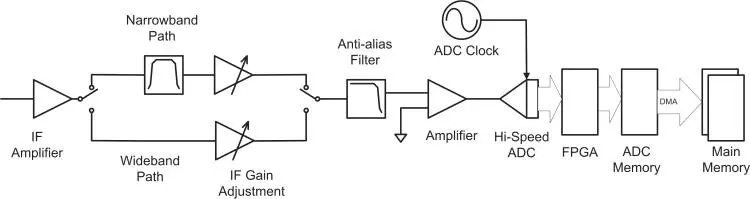
Figure 2.23 Digital IF block diagram.
The FPGA that processes the ADC readings can be configured as a digital second converter of flexible IF frequency, so the final digital IF frequency can be quite arbitrary. There are several modes of operation for the digital IF. For these high‐speed ADCs, the raw ADC readings have very high bit rates. Some of the latest designs for VNAs have four channels of data, at 16 bits and 100 mega‐samples per second to produce a data rate of 6.4 Gbps. Specialized conditioning of the signal and advanced digital signal processing (much of which is proprietary) can improve the performance of the IF ADCs to many more effective bits.
At these high data rates, the main CPU cannot process the data fast enough to keep up, so an FPGA is used to decimate and filter the signals before the processed data is sent to the main processor using shared DMA memory. The function of decimation and filtering is the basic data processing step of any digital IF; in this function, a measurement is performed by setting the source and receiver frequencies so that the first IF contains the signal of interest. The ADC samples the IF signal, typically with two to four times over sampling, although it can be as much as 60 or 100 times over sampled. A finite set of samples is processed by the FPGA to produce a final result that represents the real and imaginary parts of the signal being measured. For example, if the digital IF is operating at 100 Msps, the IF frequency is 10 MHz, and the IF filter is set to 100 kHz IF BW, then approximately 10 μs of data are captured, or approximately 1000 data samples. These 1000 samples are processed by a multiply‐add chain in the FPGA to both filter the response and extract the real and imaginary values. In this way, the 1000 samples are reduced to two samples.
A second mode of operation for the digital IF is “ADC capture” mode. In this mode, the FPGA does not process the data; rather, the data samples are simply captured into the local memory in the digital IF for a finite period of time. The entire ADC data stream is available for any further processing that might be beyond the algorithms available in the FPGA. Some modern VNAs have memory depths up to 4 Gb allowing deep memory captures. This mode of operation, while not typical, is useful for capturing anomalous effects such as transient or pulsed responses, as well as more complicated functions such as de‐modulation of IF signals.
2.2.7 Multiport VNAs
For a class of RF and microwave devices, the normal port count of two to four ports is not sufficient, and multiport measurements are required. There are two distinct classes of multiport test requirements that generate the need for two distinct RF architectures to support the measurements. In the past, RF switching test sets provide the basis for these multiport extensions, but recently true‐multiport VNAs have been introduced.
The first class of devices requires multiple sets of 2‐, 3‐, and 4‐port measurements. As such, the native mode measurements of the VNA are sufficient, and all that is required is RF switching to route the VNA ports to the various port pairs of the DUT. One example of such a DUT is a satellite multichannel‐diplexer (or multiplexer), which filters and separates signals from a common antenna path to each of several output channels, as shown in Figure 2.24. This unit has waveguide filters and interconnections to provide for the lowest possible loss.
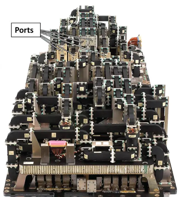
Figure 2.24 A satellite multiplexer with many outputs.
Source: Courtesy ComDev Ltd., with permission.
This device requires two‐port measurements for each path from the common port so a 2‐port VNA with one common port and one switch port can make all the required measurements. These are sometimes known as switching test sets or simple switch trees .
The second class of devices requires a measurement from each port to every other port, and in general the response of any path depends upon the loading or match applied to every other port. A “Butler matrix” is a kind of signal dividing network used in phased‐array radar systems, which has this attribute. An eight‐port Butler has four inputs and four outputs, and the proper description is an 8 × 8 S‐parameter matrix. To measure such a device, a switch matrix must be able to allow measuring every path of the device. Informally, these types of switch matrixes are called full cross‐bar switches , which implies that from the two ports of the VNA, any path of the DUT can be measured.
There is a further requirement on the Butler matrix; a full N‐by‐N port calibration measurement must be able to be performed to correct for the imperfect match of at each port. This requires not only a full cross‐bar matrix but one that supports N‐by‐N calibration as well. A third style of test set allows such N‐by‐N S‐parameters called an extension test set , which extends or adds to the number of test ports from a VNA, but these have largely been replaced with true‐multiport VNAs.
More recently, several vendors have developed high‐port‐count VNAs with up to 24 internal ports (R&S ZNBT) or configurable module multiport VNAs (Keysight M9875), in which PXI‐based VNA modules can be flexibly configured to large numbers of ports (more than 66 ports).
The various forms of multiport configurations are described next.
2.2.7.1 Switching Test Sets
Switching test sets contain only RF switches formed in a matrix to provide the needed measurement paths. Figure 2.25shows the block diagram of a simple switch tree test set. These test sets are typically constructed from either 1 × 2 RF switches or 1 × 4 to 1 × 6 RF switches. The 1 × 2 RF switches are sometimes used as some versions provide for an RF load on the unused ports. The 1 × 4 or 1 × 6 are typically mechanical switches and may not load the unused ports. If a multiport device has a path response between two ports that depends on the load match of a third port, the switch matrix must provide a load on the unused port. Larger switch configurations that have loads are often not available above 40 GHz, so 1 × 2 matrix arrays are used. Electronic 1 × 2 switches are available over a wide range of frequencies, but there are few electronic switches with higher port counts, so electronically switched test sets are typically configured from 1 × 2 RF switches.
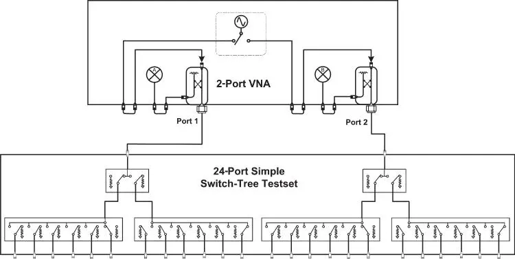
Figure 2.25 Simple switch tree test set.
The simple switch matrixes of Figure 2.25can be viewed as having a port 1 switch set and port 2 switch set, and any path from the port 1 side to the port 2 side can be measured, but no measurements are available between ports on the port 1 of the switch set, nor between ports on the port 2 side. While there are 24 ports available in the test set, only 12 paths can be measured from any one of the 12 input ports. Thus, this simple switch tree test set can support 144 paths, but a full 24 port device actually has 276 paths. There are 66 paths on the VNA port 1 side that cannot be measured, and there are 66 paths on the VNA port 2 side that cannot be measured. To obtain a full matrix of paths, a so‐called full cross‐bar switch matrix is required.
Читать дальшеИнтервал:
Закладка:
Похожие книги на «Handbook of Microwave Component Measurements»
Представляем Вашему вниманию похожие книги на «Handbook of Microwave Component Measurements» списком для выбора. Мы отобрали схожую по названию и смыслу литературу в надежде предоставить читателям больше вариантов отыскать новые, интересные, ещё непрочитанные произведения.


Обсуждение, отзывы о книге «Handbook of Microwave Component Measurements» и просто собственные мнения читателей. Оставьте ваши комментарии, напишите, что Вы думаете о произведении, его смысле или главных героях. Укажите что конкретно понравилось, а что нет, и почему Вы так считаете.