Joel P. Dunsmore - Handbook of Microwave Component Measurements
Здесь есть возможность читать онлайн «Joel P. Dunsmore - Handbook of Microwave Component Measurements» — ознакомительный отрывок электронной книги совершенно бесплатно, а после прочтения отрывка купить полную версию. В некоторых случаях можно слушать аудио, скачать через торрент в формате fb2 и присутствует краткое содержание. Жанр: unrecognised, на английском языке. Описание произведения, (предисловие) а так же отзывы посетителей доступны на портале библиотеки ЛибКат.

- Название:Handbook of Microwave Component Measurements
- Автор:
- Жанр:
- Год:неизвестен
- ISBN:нет данных
- Рейтинг книги:5 / 5. Голосов: 1
-
Избранное:Добавить в избранное
- Отзывы:
-
Ваша оценка:
Handbook of Microwave Component Measurements: краткое содержание, описание и аннотация
Предлагаем к чтению аннотацию, описание, краткое содержание или предисловие (зависит от того, что написал сам автор книги «Handbook of Microwave Component Measurements»). Если вы не нашли необходимую информацию о книге — напишите в комментариях, мы постараемся отыскать её.
Handbook of Microwave Component Measurements — читать онлайн ознакомительный отрывок
Ниже представлен текст книги, разбитый по страницам. Система сохранения места последней прочитанной страницы, позволяет с удобством читать онлайн бесплатно книгу «Handbook of Microwave Component Measurements», без необходимости каждый раз заново искать на чём Вы остановились. Поставьте закладку, и сможете в любой момент перейти на страницу, на которой закончили чтение.
Интервал:
Закладка:
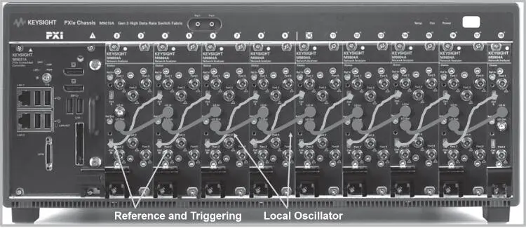
Figure 2.29 A 50‐port VNA system comprised of 6‐port and 2‐port modules.
Multiport VNAs in a modular format require the local oscillator to be shared across all modules to get the best trace noise performance. These systems provide a daisy chain approach to the connect the LO and the 10 MHz reference to each of the modules. The big advantage of a modular approach is the test system is easily reconfigured to support different test needs. For example, a 16‐port system, comprised of eight 2‐port modules, can be reconfigured into four sets of 4‐port VNAs.
While more expensive than a switched version of a VNA, the economics of a true‐multiport system readily become apparent when one considers the overall measurement time and number of sweeps needed to complete an N‐port calibrated measurement. Table 2.1shows the number of sweeps needed to complete an N‐port calibrated measurement. From a strict sweep time point of view, a true multiport VNA greatly reduces the overall test time requirement.
Table 2.1 Sweeps needed for N‐port calibration
| Total Ports | Total Paths | Switched 2‐Port | Switched 4‐Port | True Multiport |
| 8 | 28 | 56 sweeps | 24 sweeps | 8 sweeps |
| 16 | 120 | 240 sweeps | 64 sweeps | 16 sweeps |
| 24 | 276 | 552 sweeps | 144 sweeps | 24 sweeps |
2.2.7.4 Calibration of Multiport VNAs
Calibration is often a concern with multiport test systems. Traditional S‐parameter calibrations require measurements between every path of a test system. However, new techniques have greatly reduced the total number of calibration steps to the point where a full N‐by‐N port S‐parameter calibration can be achieved with a single one‐port return loss calibration and N‐1 thru measurements using the quick‐short‐open‐load‐thru (QSOLT) calibration. More details of these new calibration methods will be discussed in Chapter 3. Some manufacturers provide high‐port‐count electronic calibration modules that can simplify the calibration process.
2.2.8 High‐Power Test Systems
Most VNAs have a maximum test port operating level on the order of 10–15 dBm, with a damage level on the order of +30 dBm. Beyond the operating level, the receiver will be in substantial compression, so the data is not valid. Many VNAs provide internal receiver attenuators that allow reducing the power to the receiver, providing operation to much higher levels. The maximum input power to test port couplers are often rated higher than the maximum level of other components behind the directional‐coupler so that with proper padding and isolation, the VNA can be operated to levels as high as +43 dBm, depending on the model. Operation above these levels is possible but requires substantial external components including external couplers to ensure the power level at the VNA components is below the power damage level. Details of high power test configuration are shown in Chapter 6.
Another common practice is to add fixed attenuators between the DUT output and the VNA test port. This works well so long as the total attenuation between the test port and the DUT is less than 10 dB. Adding attenuation after the test port coupler degrades the directivity by two times the attenuation (in dB), as will be shown at the end of Section 2.3.2. In practice, up to 10 dB of external attenuation can be added and compensated for with normal calibration techniques. If between 10 and 20 dB are added, the system becomes somewhat unstable, and for more than 20 dB of added attenuation, different techniques for calibration must be used, and the S22 measurements become unreliable.
For testing devices that require high‐power drives, it is common to add an amplifier to increase the power level normally available from the VNA. One method is to simply add a booster amplifier to the port 1 output and drive the DUT directly from the booster amplifier. This generally results in poor measurements of DUT due to mismatch and gain errors in the booster amplifier. In this approach, it is common to add a booster amplifier, normalize the S21 trace, and then add the DUT and measure the resulting gain relative to the normalized booster amplifier response. However, the normalization has errors due to mismatch between the booster amplifier and the load port. And the measurement has errors due to mismatch between the booster amplifier the high‐power DUT. Further, the input match or S11 of the DUT cannot be reliably measured because booster amplifier isolation eliminates the ability to measure a signal reflected from the DUT. A second error in gain measurements often occurs with this direct approach due to gain drift or gain compression of the booster amplifier.
A better systematic approach is to add the booster amplifier behind the test port coupler, and use a second coupler as the reference‐channel tap to generate a signal proportional to the booster amplifier output signal that can be routed to the reference channel. In this scenario, a directional‐coupler rather than a power splitter is typically used to provide lower loss after the booster amplifier. The output of the reference channel is directed through the test port coupler of port 1 so that the S11 of the DUT can be accurately measured. In almost all cases, an accurate measurement of high‐drive‐power devices requires a booster amplifier followed by a reference coupler. Chapter 6provides a detailed discussion of high‐power amplifier measurements, including several alternative block diagram configurations to support various power levels.
2.2.9 VNA with mm‐Wave Extenders
Frequencies above 30 GHz are technically millimeter wave (as in they literally have a wavelength less than a cm), and it is common to consider mm‐wave above 50 GHz to over 120 GHz. At these high frequencies the losses in the test leads become so great than it often makes testing quite difficult because of the power loss from the VNA port to the DUT reference plan. This is particularly true in on‐wafer applications where the large size of the VNA means it must be placed some distance from the probes, and that means long test cables.
Thus, at these high frequencies many equipment manufacturers make mm‐wave extenders or remote heads. These heads typically have built‐in frequency multipliers for the source and LO, built‐in mixers, and built‐in directional couplers. Figure 2.30shows a representative block diagram of a mm‐wave extender. The actual implementation can vary a lot, but modern mm‐wave heads all have this similar style.
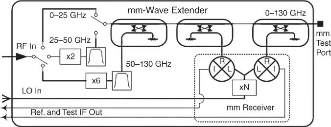
Figure 2.30 mm‐Wave Head block diagram with broadband capability.
The mm‐head shown represents a broadband head and will have a coaxial test port (typically 1 mm or smaller) that can pass DC. The low‐band path takes the RF input signal directly and passes it through to the test port. There are a couple of basic methods to provide the low‐band measurement capability: some manufacturers use the directional‐couplers in the base box (port 1, for example) to drive the RF input and will measure S‐parameters from low frequency to the first multiplier band using the normal VNA receivers in the base box. This reduces the need for broadband couplers in the head but may add instability due to the long test port cables from the base box to the mm‐input. One manufacturer uses broadband receivers in the mm‐receiver portion of the head, as well as broadband coupler. The RF signal is only a source, and even at low frequency the mm‐head couplers are used. This provides a quite stable result, but it is a difficult design to achieve such a broadband coupler. The LO multiplier either can be a discrete multiplier or can rely on higher‐order harmonic conversion in the mixer. The reference and test IF signals are returned to the base box where they are processed to produce the desired detection.
Читать дальшеИнтервал:
Закладка:
Похожие книги на «Handbook of Microwave Component Measurements»
Представляем Вашему вниманию похожие книги на «Handbook of Microwave Component Measurements» списком для выбора. Мы отобрали схожую по названию и смыслу литературу в надежде предоставить читателям больше вариантов отыскать новые, интересные, ещё непрочитанные произведения.


Обсуждение, отзывы о книге «Handbook of Microwave Component Measurements» и просто собственные мнения читателей. Оставьте ваши комментарии, напишите, что Вы думаете о произведении, его смысле или главных героях. Укажите что конкретно понравилось, а что нет, и почему Вы так считаете.