Joel P. Dunsmore - Handbook of Microwave Component Measurements
Здесь есть возможность читать онлайн «Joel P. Dunsmore - Handbook of Microwave Component Measurements» — ознакомительный отрывок электронной книги совершенно бесплатно, а после прочтения отрывка купить полную версию. В некоторых случаях можно слушать аудио, скачать через торрент в формате fb2 и присутствует краткое содержание. Жанр: unrecognised, на английском языке. Описание произведения, (предисловие) а так же отзывы посетителей доступны на портале библиотеки ЛибКат.

- Название:Handbook of Microwave Component Measurements
- Автор:
- Жанр:
- Год:неизвестен
- ISBN:нет данных
- Рейтинг книги:5 / 5. Голосов: 1
-
Избранное:Добавить в избранное
- Отзывы:
-
Ваша оценка:
Handbook of Microwave Component Measurements: краткое содержание, описание и аннотация
Предлагаем к чтению аннотацию, описание, краткое содержание или предисловие (зависит от того, что написал сам автор книги «Handbook of Microwave Component Measurements»). Если вы не нашли необходимую информацию о книге — напишите в комментариях, мы постараемся отыскать её.
Handbook of Microwave Component Measurements — читать онлайн ознакомительный отрывок
Ниже представлен текст книги, разбитый по страницам. Система сохранения места последней прочитанной страницы, позволяет с удобством читать онлайн бесплатно книгу «Handbook of Microwave Component Measurements», без необходимости каждый раз заново искать на чём Вы остановились. Поставьте закладку, и сможете в любой момент перейти на страницу, на которой закончили чтение.
Интервал:
Закладка:
2.2.3.2 Step Attenuator Effects
In some VNA designs, a step attenuator is added between the reference coupler and the test coupler to allow a greater change in the source power setting beyond that which the source ALC circuit can produce. This step attenuator has the additional benefit of providing a good match to the test port. In cases where the power source‐match and ratio source‐match are not the same, the step attenuator reduces the difference between these values based on twice the attenuation value. Reducing the difference between power source‐match and ratio source‐match allows one to compute the error in source power from the ratio source‐match, which is determined as part of the normal calibration process. In general, the power source‐match is not characterized during any normal calibration.
Another issue to be concerned about with step attenuations is their effect on the quality of the measurement when the attenuation value is changed. In most newer VNAs, the nominal attenuator value is known, and the effective value of the reference receiver is compensated for when the attenuator value is changed. The source ALC power is also changed, so that changing the attenuator value causes only a slight change in the value of the power coming from the test port; the nominal attenuator value is usually within 0.25–0.5 dB of the actual attenuator value. Since the port power stays the same, the internal source power must be raised by the amount of increase in the step attenuator. Since the reference receiver comes before the step attenuator, it will see a larger signal value; as it is desired to have the reference receiver power display the same value as the port power, its reading is also decreased by the value of the step attenuator.
Placing the step attenuator at this point in the block diagram has a distinct advantage in that it allows a large signal in the reference channel even when a small signal is needed at the test port, providing a low noise signal.
The loss of the step attenuator is well compensated for, but its effect on the match is not. If the preset condition has the step attenuator set to 0 dB, the match of the port is terminated back in the test port switch. When even a single stage of test port attenuation is used, the predominate source and load match characteristic is set by the match of the attenuator, which is typically quite good. Thus, it is good practice to use some source step attenuation if the maximum test port power is not required for the measurement. And since the raw match is better for any attenuator setting other than the 0 dB step, the effect on a calibrated measurement if the attenuator is switched to a different, non‐zero, value is smaller if the calibration is performed with some attenuation applied.
Some older VNAs did not allow changing the attenuation value after calibration and did not compensate for the nominal value of an attenuator change; error correction in these VNAs is often turned off for a step attenuator change.
In general, changing a step attenuator will change all the raw error terms on the port that has the step attenuator. Techniques are discussed in Chapter 3that can compensate for much of this change.
2.2.3.3 Test Set Reflections
In addition to the source‐match effects produced by the source impedance, power source‐match, and ratio source‐match, reflections from within the test set of the VNA will also exist, as well as from the test port cables and from any fixtures that provide an interface from the VNA to the DUT. These sources of mismatch are common to all of the previously mentioned source‐match effects and will add to them in a similar way. However, since they are common, their effects on port power and gain are also the same.
The reflection and mismatch between the reference channel split and the test port coupler affect the incident signal, a1 , but are not monitored by the reference channel receiver. Reflections after the test port coupler also affect the a1 signal but will be apparent in changes measured on the reflected signal, b1 . However, their composite effect will add to the overall source‐match, and their effects on measurements can be compensated provided they remain stable. In addition, mismatch and loss after the test port coupler can be characterized in such a way that changes to these values, such as due to drift in a test port cable, also can be compensated in some cases. Mismatch correction in power measurements is discussed in detail in Chapter 3.
2.2.4 Directional Devices
One vital VNA component is the directional device used at the test port to separate the reflected wave from the incident wave. This is most often a directional‐coupler or directional bridge, although simpler structures have been proposed as well. These devices are characterized by their main‐line loss (the attenuation of the a1 signal), the coupled‐arm loss (the attenuation of the b1 signal), and their directivity (the ability to separate the b1 signal from the a1 signal). In addition, any mismatch in the directional device will contribute to the port match and source‐match. If there is mismatch before the directional device, it will have no effect on its directional characteristics (directivity or isolation). However, any mismatch after the directional device, such as in a test port cable or fixture, will contribute equally to mismatch and degradation of directivity, as described in Section 1.10.
2.2.4.1 RF Directional Bridges
Most RF VNAs make use of a directional bridge, which has the important characteristic of maintaining good coupling and isolation over very wide frequency ranges and at very low frequencies. While the most common implementation of a bridge is a balanced Wheatstone bridge, this simple implementation can be modified to create a component that has characteristics similar to a directional‐coupler, but with much wider frequency range and low frequency of operation. A bridge is often used in metrology applications where balance in a DC resistive path provides a measure of some quantity such as the power absorbed by a load (see Section 1.15). To understand how these bridges can be configured as directional‐couplers, with low loss and high isolation, consider the diagram in Figure 2.12, which is a common representation of a Wheatstone bridge.
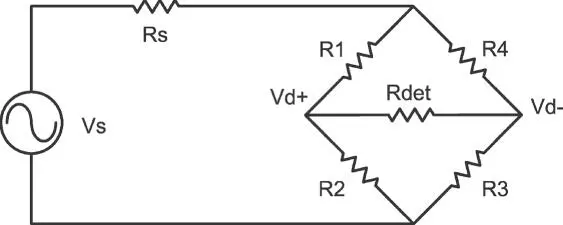
Figure 2.12 Schematic of a directional bridge.
In this configuration, the signal from the source is applied across the top and bottom of the bridge, and if the ratio of R1/R2 is equal to R4/R3, the net voltage across Rdet (which in a common bridge represents the meter movement) will be zero, and no current will flow through the detector.
In a thermistor, all the resistors are 50 Ω, and one of them represents the RF input of the power sensor, typically R3. A DC signal is applied from the source across the bridge, and the imbalance is measured as the voltage difference across the Rdet resistor. In an RF bridge it is desired to isolate the bottom node of the bridge from ground, and so a transformer is added for this purpose, as shown in Figure 2.13. This 1:1 transformer performs the function of a BALanced‐UNbalanced transformer (or balun), changing the unbalanced (or grounded) source into a balanced signal across the bridge. Doing this allows grounding a different leg of the bridge, which as will be seen is key to making a bridge act as a directional‐coupler.
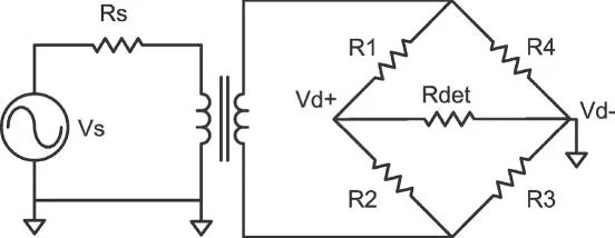
Figure 2.13 Adding a transformer between the source and the bridge.
Читать дальшеИнтервал:
Закладка:
Похожие книги на «Handbook of Microwave Component Measurements»
Представляем Вашему вниманию похожие книги на «Handbook of Microwave Component Measurements» списком для выбора. Мы отобрали схожую по названию и смыслу литературу в надежде предоставить читателям больше вариантов отыскать новые, интересные, ещё непрочитанные произведения.


Обсуждение, отзывы о книге «Handbook of Microwave Component Measurements» и просто собственные мнения читателей. Оставьте ваши комментарии, напишите, что Вы думаете о произведении, его смысле или главных героях. Укажите что конкретно понравилось, а что нет, и почему Вы так считаете.