Joel P. Dunsmore - Handbook of Microwave Component Measurements
Здесь есть возможность читать онлайн «Joel P. Dunsmore - Handbook of Microwave Component Measurements» — ознакомительный отрывок электронной книги совершенно бесплатно, а после прочтения отрывка купить полную версию. В некоторых случаях можно слушать аудио, скачать через торрент в формате fb2 и присутствует краткое содержание. Жанр: unrecognised, на английском языке. Описание произведения, (предисловие) а так же отзывы посетителей доступны на портале библиотеки ЛибКат.

- Название:Handbook of Microwave Component Measurements
- Автор:
- Жанр:
- Год:неизвестен
- ISBN:нет данных
- Рейтинг книги:5 / 5. Голосов: 1
-
Избранное:Добавить в избранное
- Отзывы:
-
Ваша оценка:
Handbook of Microwave Component Measurements: краткое содержание, описание и аннотация
Предлагаем к чтению аннотацию, описание, краткое содержание или предисловие (зависит от того, что написал сам автор книги «Handbook of Microwave Component Measurements»). Если вы не нашли необходимую информацию о книге — напишите в комментариях, мы постараемся отыскать её.
Handbook of Microwave Component Measurements — читать онлайн ознакомительный отрывок
Ниже представлен текст книги, разбитый по страницам. Система сохранения места последней прочитанной страницы, позволяет с удобством читать онлайн бесплатно книгу «Handbook of Microwave Component Measurements», без необходимости каждый раз заново искать на чём Вы остановились. Поставьте закладку, и сможете в любой момент перейти на страницу, на которой закончили чтение.
Интервал:
Закладка:
Figure 2.1shows the block diagram of a TR system. For simplicity sake the reference receiver will be normally at port 1, measuring the a1 wave, and the test receivers were limited to the two ports as well; normally the test receiver at port 1 is the reflection receiver ( b1 ), and the test receiver at port 2 is the transmission receiver ( b2 ). The source is typically split using a two‐resistor power splitter or a coupler to create a reference signal that is proportional to the incident signal on the DUT, followed by a directional‐coupler or directional bridge, whose coupled arm goes to the reflection test receiver, measuring b1 . After the DUT, the transmission test receiver measures b2 . Because of advances in VNAs and integration of dual reflectometers and receivers, this architecture is seldom seen in modern VNAs.
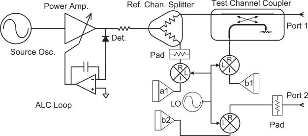
Figure 2.1 A TR network analyzer block diagram.
A full S‐parameter system extends the block diagram of the TR system by adding a reflectometer at each port and provides a source at each port. Older systems would switch the source between the ports using a test port switch. Two such block diagrams are shown in Figure 2.2. There are two distinct versions that use either one or two reference receivers.
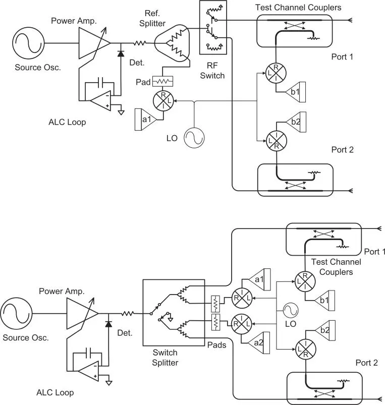
Figure 2.2 S‐parameter block diagrams for a three‐receiver and four‐receiver VNA.
The three‐receiver version (upper diagram) was common in lower‐cost or RF network analyzers in the past but has largely been replaced with four receiver versions. Having individual receivers for all the reference and test port channels provides for more and better calibration choices, as will be discussed in Chapter 3.
Older analyzers such as the HP‐8510 used separate external sources and switched the source between the ports; others had internal sources, but the cost of the source was a major portion of the instrument cost, so a single switched‐source was used in these integrated analyzers. Often, the reference channel splitter was integrated into this switch as well. This provided a compact switch‐splitter assembly and allowed a lower‐cost alternative to individual splitters or directional‐couplers.
Modern network analyzers make use of a hybrid approach with two or more internal sources, such that more than one port at a time can have an output signal, as shown in Figure 2.3.
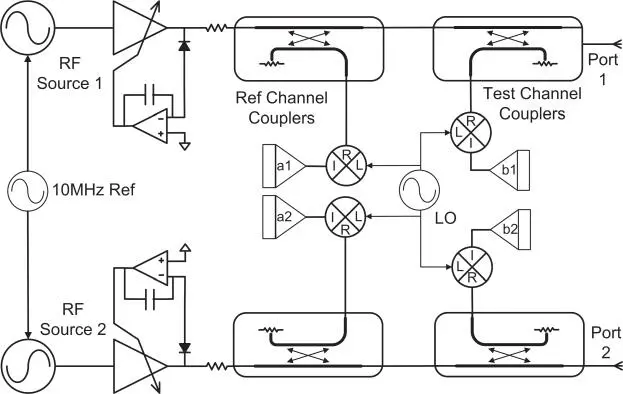
Figure 2.3 Multiple sources in a single VNA.
While there is no requirement for having more than one port active in traditional S‐parameter measurements, advanced measurements such as two‐tone intermodulation distortion (IMD), active‐load, or differential‐device test can make good use of these extra sources. In these systems it is common to use a directional‐coupler in both the reference and test arms for lower loss from the source to the test port, allowing higher maximum test port power. One synthesizer (that is, the frequency generation unit) may be shared between two ports (of a 4‐port VNA) with an individual output amplifier and leveling circuits available at each of the ports. This system can provide outputs at any of the ports at the same time or provide two different frequencies out of pairs of ports, which is useful for mixer test applications.
2.2.1 VNA Source
The VNA source provides the stimulus for the S‐parameter measurement. In the original VNAs these were open‐loop sweepers, but since about 1985 the use of frequency synthesizers has become the norm. Sweepers used open‐loop swept‐frequency oscillators to produce the stimulus signals; synthesizers replaced the open‐loop control with fractional‐N or multi‐loop signal generation where the output signal is digitally derived from a 10 MHz reference oscillator to a resolution of less than 1 Hz. Early sources were routed directly to the test sets of VNAs, which were also external, stand‐alone instruments, often with the first converter assembly inside.
More recently the source is provided internally to the VNA. In the first integrated VNAs, the signal quality of the internal source was less than that of external instrumentation sources but had the advantage of being much faster in sweeping frequency. For applications such as filter tuning and test, fast sweep times across wide frequency ranges were required. Common to VNA sources are the ability to vary power level over a prescribed range, usually called the automatic‐level‐control (ALC) range, which has values from 20 to over 40 dB. These ranges are often extended with integrated discrete step‐attenuators after the source. With new open‐loop control, the power range can be extended even farther, typically greater than 70 dB.
Most VNA sources also have a power flatness specification to provide some constant power to the DUT. In many cases, this level is digitally corrected by a factory calibration to be quite accurate at the test port. In addition, a user‐performed source‐power‐level correction is usually available to provide additional accuracy enhancement, as described later in Chapter 3.
A typical VNA source block diagram is shown in Figure 2.4.
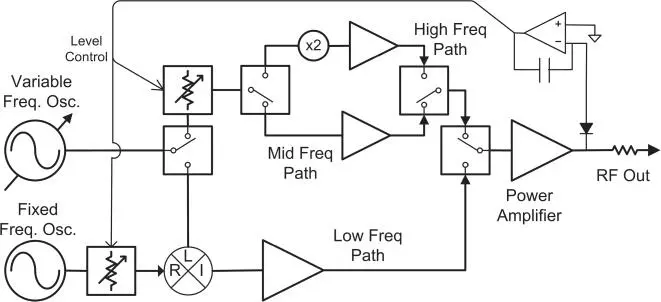
Figure 2.4 Example of a VNA source block diagram.
Generally, there is a fundamental oscillator that provides a swept frequency response over one or more octaves. Previously, the output was often switched or split to use as an local oscillator (LO) to a low‐frequency heterodyne source stage; many modern VNAs use direct digital synthesis to get the low‐frequency response and divide the fundamental oscillator to get the higher range of the low‐frequency path.
The swept frequency oscillator is typically phase‐locked to a lower‐frequency fractional‐N (F.N) circuit or direct‐digital synthesizers (DDSs). In older VNAs, the phase locking was accomplished through the reference receiver, which reduced cost but required that the reference path signal remain present for all measurements. Modern analyzers separate the frequency synthesis for sources from receivers for greater flexibility and no longer require the any signal be present in the reference path. Because of this, the RF signal may be pulsed modulated without losing phase lock on the synthesizer.
The output may also go to multiple stages of division or multiplication, followed by amplification and filtering. The final output signal is combined from each of the input signals, resulting in broad frequency coverage. Typically, this common output has some RF detector on it to provide for ALC loop operation, maintaining constant source power over the different frequency bands and compensating for amplifier flatness. But often the ALC attenuator drive can be operated in an open‐loop mode to extend the power range beyond that of the detector diode.
The level control circuits often use an amplitude modulator before the amplification chain to complete the ALC loops. In some modern VNAs, a pulse modulator is added as well to provide for high‐speed pulsed RF measurements. When a pulse‐modulator is used inside the ALC loop, the ALC function must be disabled as it will attempt to respond to the pulsed signals. In this open‐loop mode, more sophisticated calibration or digital control must be used to control the source output power. Recently the use of a reference or test receiver as the ALC loop power control, rather than the internal diode detector, has become more common. This form of receiver leveling provides accurate results if the receivers are calibrated, a much wider range of leveling than the diode detector can support, and the ability to be programmatically controlled to correct for any external path loss or to provide a prescribed power profile.
Читать дальшеИнтервал:
Закладка:
Похожие книги на «Handbook of Microwave Component Measurements»
Представляем Вашему вниманию похожие книги на «Handbook of Microwave Component Measurements» списком для выбора. Мы отобрали схожую по названию и смыслу литературу в надежде предоставить читателям больше вариантов отыскать новые, интересные, ещё непрочитанные произведения.


Обсуждение, отзывы о книге «Handbook of Microwave Component Measurements» и просто собственные мнения читателей. Оставьте ваши комментарии, напишите, что Вы думаете о произведении, его смысле или главных героях. Укажите что конкретно понравилось, а что нет, и почему Вы так считаете.