Fundamentals of Terahertz Devices and Applications
Здесь есть возможность читать онлайн «Fundamentals of Terahertz Devices and Applications» — ознакомительный отрывок электронной книги совершенно бесплатно, а после прочтения отрывка купить полную версию. В некоторых случаях можно слушать аудио, скачать через торрент в формате fb2 и присутствует краткое содержание. Жанр: unrecognised, на английском языке. Описание произведения, (предисловие) а так же отзывы посетителей доступны на портале библиотеки ЛибКат.

- Название:Fundamentals of Terahertz Devices and Applications
- Автор:
- Жанр:
- Год:неизвестен
- ISBN:нет данных
- Рейтинг книги:4 / 5. Голосов: 1
-
Избранное:Добавить в избранное
- Отзывы:
-
Ваша оценка:
Fundamentals of Terahertz Devices and Applications: краткое содержание, описание и аннотация
Предлагаем к чтению аннотацию, описание, краткое содержание или предисловие (зависит от того, что написал сам автор книги «Fundamentals of Terahertz Devices and Applications»). Если вы не нашли необходимую информацию о книге — напишите в комментариях, мы постараемся отыскать её.
Fundamentals of Terahertz Devices and Applications
Fundamentals of Terahertz Devices and Applications — читать онлайн ознакомительный отрывок
Ниже представлен текст книги, разбитый по страницам. Система сохранения места последней прочитанной страницы, позволяет с удобством читать онлайн бесплатно книгу «Fundamentals of Terahertz Devices and Applications», без необходимости каждый раз заново искать на чём Вы остановились. Поставьте закладку, и сможете в любой момент перейти на страницу, на которой закончили чтение.
Интервал:
Закладка:
The last step of the process consists of applying an antireflective coating to the lens which is essential to reduce the high reflection losses that occur by using a dielectric with high permittivity. A coating with the polymer Parylene is usually employed as matching layer at submillimeter‐wave frequencies.It has an index of refraction around 1.64, which is not the ideal for silicon, but it is close enough to considerably reduce the reflections. The coating conformal is deposited using vapor deposition which allows high control of the thickness and uniformity.
2.5.1.2 Surface Accuracy
The fabricated surface of the lens can be analyzed independently of the rest of the antenna by the accurate characterization of the actual fabricated surface. Surface profilometers are used to map the 3D profile of the lens surface with high resolution. The basic parameters of this surface in terms of radius R , diameter of the aperture D , height H are computed with an optimization procedure using, for example, the optimization toolbox in Matlab and a basic cost function to minimize. The cost function compares the fabricated surface and an ideal spherical surface until it finds the best fitting sphere. By evaluating the error between both surfaces we can have a sense of how spherical the fabricated lens is, and identify flaws that can improve the fabrication process. For example, Figure 2.25a shows the profile of a fabricated shallow lens of D = 2.6 mm measured with a profilometer and its error surface obtained when compared with a perfect sphere. In this case, since the edges of the lens did not provide a good fit with the sphere, an improvement of the performance could be achieved by adjusting the illumination to minimize the lens area illuminated. This adjustment can be achieved by decreasing the lens thickness W , which will decrease the illumination of the lens edges, i.e. increase the edge field taper.
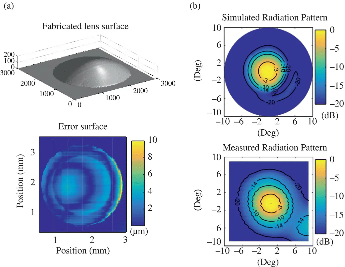
Figure 2.25(a) Surface measured of the fabricated lens of D = 2.6 mm. The error surface defined as the difference between the measured surface and a perfect sphere is shown underneath. (b) Computed radiation pattern of the measured lens surface and the measured radiation pattern of the whole lens antenna at 1.9 THz from [26].
One can have an estimation of the effects of the aberrations in the radiation pattern by translating the error surface into a phase error surface. We can assume that the field distribution on top of the aperture has a Gaussian field distribution of a certain taper, for example −14 dB, with a phase of  , where
  is the distance from the phase center of the waveguide feed to the fabricated lens surface and
  is the distance from the fabricated lens surface to the lens aperture plane. The resulting radiation pattern is obtained by calculating the Fourier transform of this resulting field distribution. From these fields, the directivity and Gaussicity loss can be computed to have a sense of how our antenna would perform. In this example, the small lens of 2.6 mm aperture would result in a directivity loss of 0.2 dB and a Gaussicity loss close to 2%. Figure 2.25b shows the radiation patterns of the fabricated lens at 1.9 THz for a 2.6 mm diameter lens using the method explained compared with the measured radiation pattern.
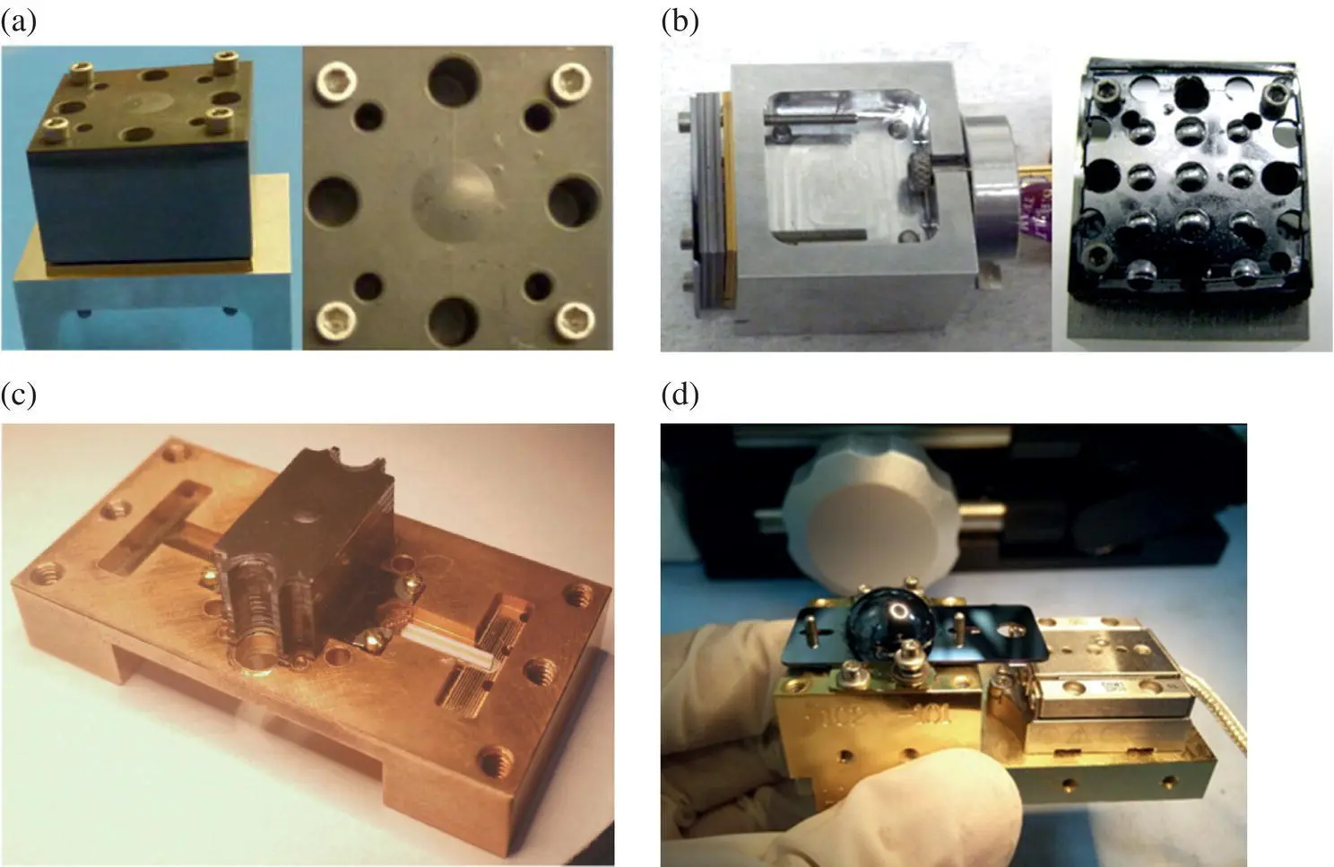
Figure 2.26Photographs of different lens antenna prototypes fed by leaky‐wave feeds (a) at 550 GHz with lens laser micro‐machined [33].
Source : Alonso‐DelPino et al. [33]; IEEE.
(b) At 550 GHz with lens fabricated using DRIE silicon micromachining [25].
Source : Llombart et al. [25]; IEEE.
(c) At 1.9 THz integrated with tripler all in silicon micromachining package [26].
Source : Alonso‐delPino et al. [26]; IEEE.
(d) At 550 GHz integrated with a piezo‐electric motor in order to perform beam‐scanning [48].
Source : Alonso‐delPino et al. [48]; IEEE.
2.5.2 Examples of Fabricated Antennas
In this section, we will show different example implementations of leaky‐wave antennas feeding silicon lenses. Figure 2.18shows the photograph of the different prototype examples we will comment on.
Figure 2.26a and b show two prototypes of leaky‐wave microlens antennas fabricated at 550 GHz. The first lens was fabricated using laser micromachining, while the second lens was fabricated using DRIE silicon micromachining. Even though both antennas obtained a good agreement with the expected results, the DRIE silicon micromachined lens portrayed some aberrations that were visible in in the radiation pattern measurements showing an increase in the secondary lobes and a small tilt.
Figure 2.26c shows a microlens antennas at 1.9 THz integrated with a 1.9 THz Schottky‐based tripler all in the same wafer. The antenna was synthesized on 12 resistivity silicon wafers and the tripler waveguide circuit was synthesized on three wafers. All the wafers, including the lenses, were fabricated using DRIE silicon micromachining process, aligned using the silicon compressive pin technique, and finally glued together. An alignment better than 2 μm was achieved across the wafer stack [26]. Even though in this case, the lenses suffered from aberrations caused by the lack of the surface control in the fabrication process, well‐focused beam patters very similar to the design ones were achieved.
On another note, new efforts are now being investigated to enable lens beam‐scanning capabilities in the system front end. Figure 2.26d shows a highly integrated beam scanning lens‐antenna using a piezo‐electric motor demonstrated operating at 550 GHz presented in [48]. A hemispherical lens was glued on top of a silicon wafer containing alignment marks processed using DRIE silicon micromachining. The piezoelectric motor displaced the lens around ±1 mm from the center position of the lens, providing a beam scan of ±25°. Not only this method can be employed for improving the alignment of the lens with the feed, but it also has the potential to enable beam‐scanning capabilities on the system front end for future terahertz imaging systems.
The results achieved so far show a great potential to use these dielectric lens antennas in the development of future focal plane arrays at terahertz frequencies. By using the leaky‐wave waveguide feed, we only need a small part of the surface of the lens, which reduces the reflection losses and phase errors that these type of lenses suffer. But most of all, it allows the use of photolithographic process when fabricating the lens. The fabrication of the lenses using photolithographic process reduces the cost, with the same performance achieved with other fabrication methods, such as laser micromachining.
Exercises
E2.1 Derivation of the Transmission Coefficients and Lens Critical Angle
In Section 2.2, we defined the Fresnel reflection coefficients τ ⊥( Q ), τ ∥( Q ) as:
Читать дальшеИнтервал:
Закладка:
Похожие книги на «Fundamentals of Terahertz Devices and Applications»
Представляем Вашему вниманию похожие книги на «Fundamentals of Terahertz Devices and Applications» списком для выбора. Мы отобрали схожую по названию и смыслу литературу в надежде предоставить читателям больше вариантов отыскать новые, интересные, ещё непрочитанные произведения.


Обсуждение, отзывы о книге «Fundamentals of Terahertz Devices and Applications» и просто собственные мнения читателей. Оставьте ваши комментарии, напишите, что Вы думаете о произведении, его смысле или главных героях. Укажите что конкретно понравилось, а что нет, и почему Вы так считаете.