Fundamentals of Terahertz Devices and Applications
Здесь есть возможность читать онлайн «Fundamentals of Terahertz Devices and Applications» — ознакомительный отрывок электронной книги совершенно бесплатно, а после прочтения отрывка купить полную версию. В некоторых случаях можно слушать аудио, скачать через торрент в формате fb2 и присутствует краткое содержание. Жанр: unrecognised, на английском языке. Описание произведения, (предисловие) а так же отзывы посетителей доступны на портале библиотеки ЛибКат.

- Название:Fundamentals of Terahertz Devices and Applications
- Автор:
- Жанр:
- Год:неизвестен
- ISBN:нет данных
- Рейтинг книги:4 / 5. Голосов: 1
-
Избранное:Добавить в избранное
- Отзывы:
-
Ваша оценка:
Fundamentals of Terahertz Devices and Applications: краткое содержание, описание и аннотация
Предлагаем к чтению аннотацию, описание, краткое содержание или предисловие (зависит от того, что написал сам автор книги «Fundamentals of Terahertz Devices and Applications»). Если вы не нашли необходимую информацию о книге — напишите в комментариях, мы постараемся отыскать её.
Fundamentals of Terahertz Devices and Applications
Fundamentals of Terahertz Devices and Applications — читать онлайн ознакомительный отрывок
Ниже представлен текст книги, разбитый по страницам. Система сохранения места последней прочитанной страницы, позволяет с удобством читать онлайн бесплатно книгу «Fundamentals of Terahertz Devices and Applications», без необходимости каждый раз заново искать на чём Вы остановились. Поставьте закладку, и сможете в любой момент перейти на страницу, на которой закончили чтение.
Интервал:
Закладка:
The micromachining techniques used for the fabrication of heterodyne receivers and sources at submillimeter‐wave frequencies are based on CNC metal block machining, as well as wafer‐level processing using photolithographic techniques. Compared with metal block machining, wafer‐level processing allows a higher integration of the whole receiver, which reduces the volume, mass, and losses. The different waver level processing solutions in literature, from the use of SU‐8 [36] machining to lithography, electroplating, and molding (LIGA)‐based processes [37] that use thick resist and electroplating processes to form the waveguide walls, suffer from limitations in terms of multi‐etching capabilities and non‐uniformity problems. Silicon micromachining based on DRIE allows the fabrication of high aspect ratio features while maintaining straight sidewalls and smooth multi‐depth surfaces. This technology is very attractive for the development of heterodyne receivers and sources as the technology allows the fabrication of complex circuit features that require multiple waveguides of various depths, especially as the wavelength decreases, when machining tolerances become a concern.
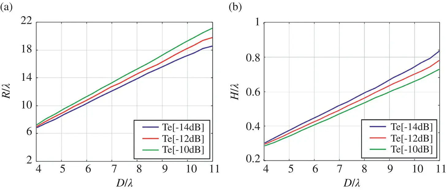
Figure 2.20(a) Radius R and (b) height H of the lens as a function of the diameter D for different field tapers.
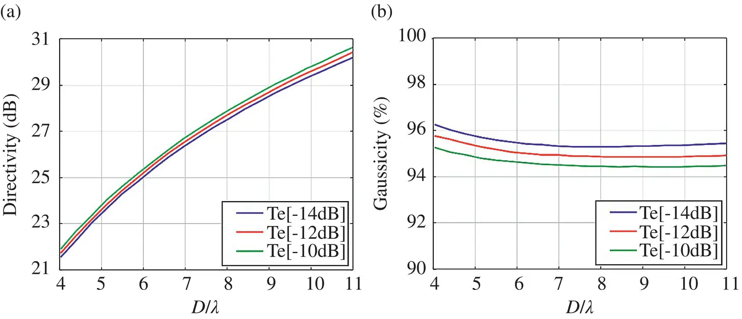
Figure 2.21(a) Directivity and (b) Gaussicity achieved for the shallow lens antenna Reflection coefficient centered at a central frequency f for the dimensions shown in the table.
As previously stated, the presented antenna composed by a leaky‐wave feed and the shallow lens can be fabricated in four silicon wafers using DRIE processes. The first wafer consists of the iris and the waveguide feature. The second wafer contains the air cavity. The third wafer contains dummy silicon wafer to achieve the correct lens thickness. The fourth wafer contains the lens surface. The four different wafers (i.e. iris air gap, bulk wafers, and lens) will be assembled together on a single wafer stack. Note that high resistivity silicon wafers, i.e. 10 kΩ cm, are required to reduce the dielectric absorption loss. And, the wafers need to be double‐sided polished in order to have good surface contact between all the wafers in the stack, avoiding air gaps. The alignment, which is a challenge when working at such high frequencies, has been solved by using a silicon compressive pin that is slightly larger than the pocket and can be compressed slightly when put into place [26].
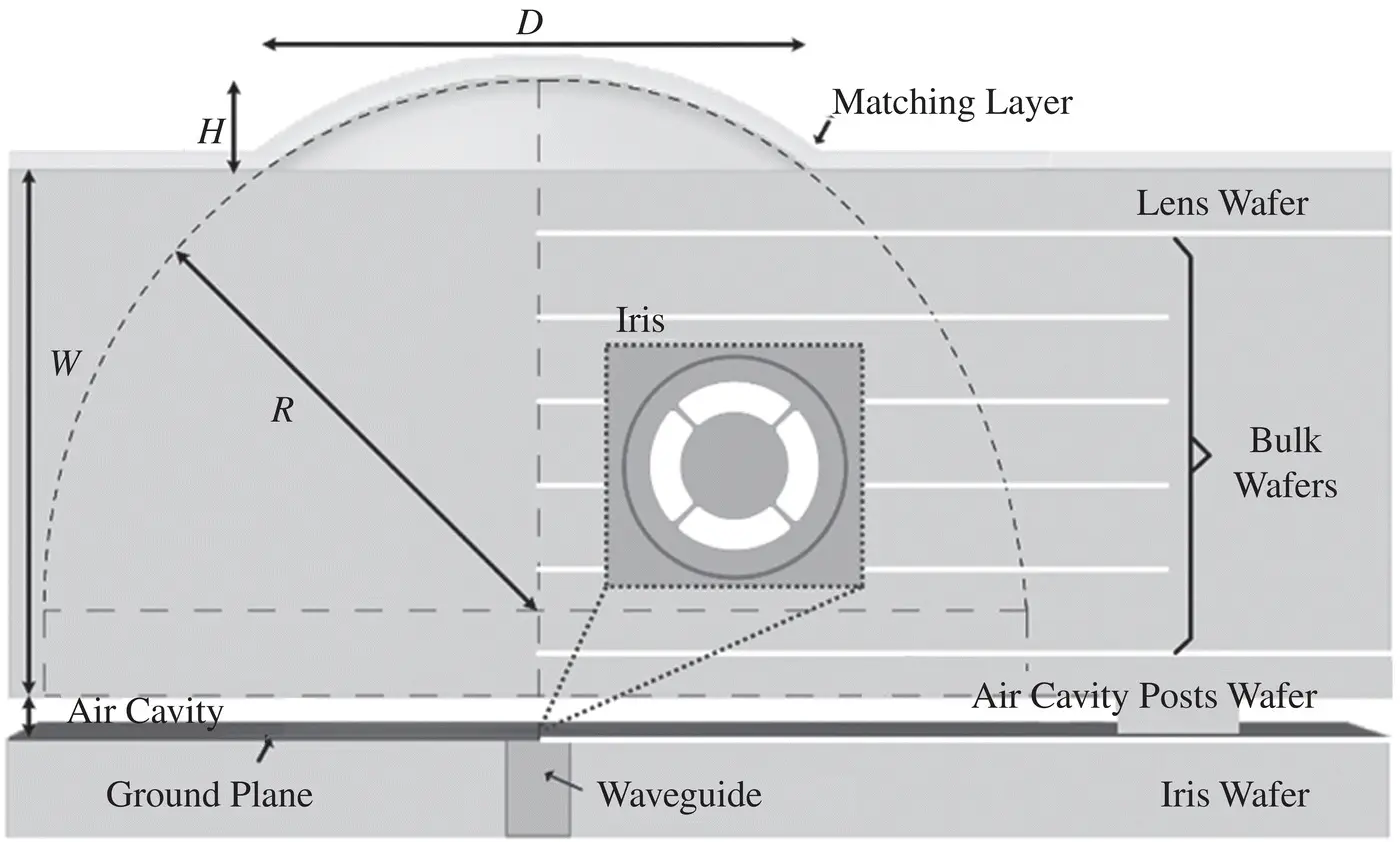
Figure 2.22Reflection coefficient centered at a central frequency f for the dimensions shown in the table.
2.5.1 Silicon DRIE Micromachining Process at Submillimeter‐wave Frequencies
In order to achieve the depth accuracy and smoothness of the features on silicon, Silicon‐on‐insulator (SOI) wafers are commonly employed, since thin layers of SiO 2act as etch stops of the silicon. For example, [26] presented an iris of the leaky‐wave antenna at 1.9 THz fabricated on a 2.5 μm silicon membrane. Compared with a thermal oxide membrane, the crystalline silicon provides more robustness to compressive stress. In that case, a SOI wafer with a 2 μm device layer was used because, together with the metallization, the membrane would reach the desired 2.5 μm. And a handling wafer of 400 μm defined the waveguide on the back of the membrane.
The step by step fabrication of the slot iris and waveguide process is shown in Figure 2.23. Thermally grown SiO 2is used as a hard mask in the front and back of the SOI wafer. Since the small size of the double slot iris, an i‐line Canon stepper is used to illuminate the SiO 2. And for the rest of the waveguide and alignment features, regular UV photolithography can be employed. The pre‐etching of the features, i.e. the slot iris and the waveguide, on the front and back of the SiO 2layer are performed using photoresist and an inductively coupled plasma (ICP) reactive ion etcher. Then, the silicon on the front backside is etched using a PlasmaTherm DRIE system. While the selectivity of the silicon to photoresist is around 70 : 1, the selectivity of the silicon to SiO 2can be optimized to reach 130 : 1, which allows to etch high depth features with high control. The SiO 2was removed using a hydrogen fluoride HF solution.
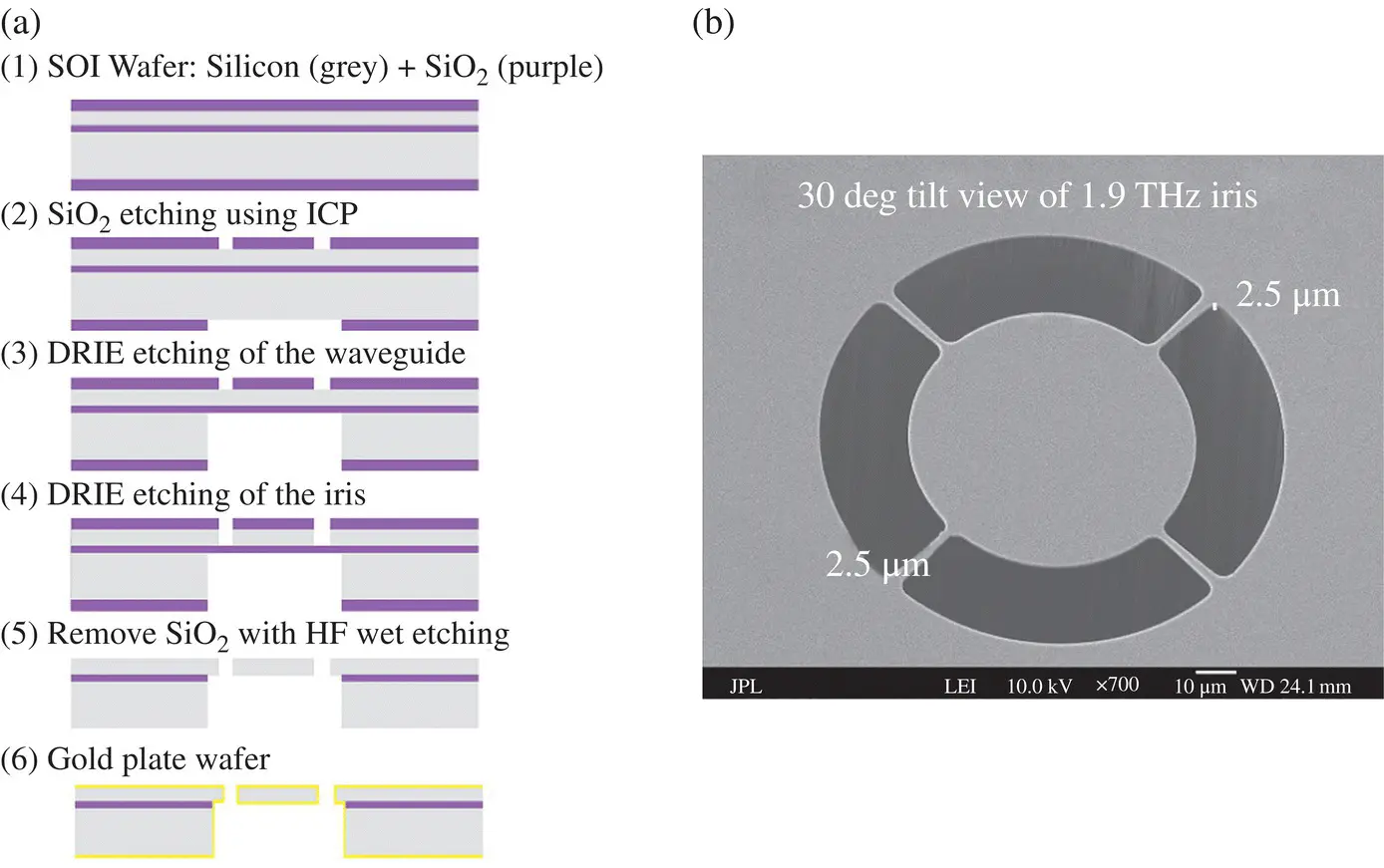
Figure 2.23(a) Sketch of the membrane fabrication process that contains the iris and waveguide of the leaky‐wave feed. (b) SEM of the iris developed at 1.9 THz in [26] using the explained process.
Source : Alonso‐delPino et al. [26]; IEEE.
At the end of the process, the overall wafer was sputtered with gold, used due to its high conductivity, immunity to oxidation, and ease of deposition. The overall results of this process can be observed in the scanning electron microscope (SEM) image in Figure 2.23b, showing a very clean and well‐defined pair of double slots.
The rest of the wafers that define the lens are processed similarly as the procedure described but, because the radiation is going through the wafers, it is necessary the use of high resistivity silicon wafers (the resistivity around 10 kΩ cm) to avoid the introduction of absorption losses.
2.5.1.1 Fabrication of Silicon Lenses Using DRIE
Silicon shallow lens arrays have been fabricated either by laser micro‐machining process or using photolithographic processes based on DRIE. Laser micro‐machining allows the fabrication of 3‐D geometries with accuracy as presented in [33], however, it is a linear process where the cost depends on the laser time, which might not be the most cost‐efficient method for large lens arrays. A novel DRIE silicon process presented in [47] allows the fabrication of arrays of lenses on a single wafer and in parallel. This section will provide an overview of the process and a fast method to estimate the overall fabrication accuracy without needing to test the lens antenna.
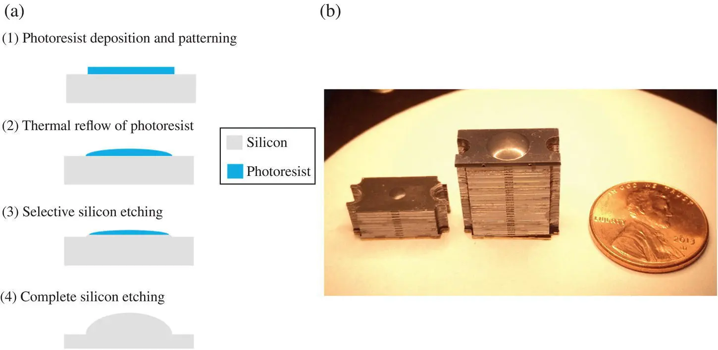
Figure 2.24(a) Sketch of the fabrication process of the shallow silicon lens. (b) Photograph of shallow lens antennas at 1.9 THz of diameter 2.6 and 6.3 mm presented in [26].
Source : Alonso‐delPino et al. [26]; IEEE.
The process to fabricate the silicon shallow lens consists of four steps, illustrated in Figure 2.24a. The first step consists of the patterning of the photoresist on a high resistivity wafer with the desired lens aperture diameter. The thickness and aperture diameter of the photoresist applied onto the silicon wafer defines the thickness and curvature of the lens surface. Multiple photoresist coatings can be applied to achieve the desired thickness. Next, the photoresist reflows by applying heat, i.e. around 110 °C on a hot plate, to the wafer. The surface tension applied to the photoresist by its coating above the glass transition temperature, makes the surface reflow into a spherical shape. Last, the photoresist shape is transferred into the silicon wafer using a DRIE process. The photoresist and silicon etching selectivity, controlled by the CF 4and O 2gas ratio and the DC and RF power applied in the process, defines the curvature of the overall lens. The examples shown below a selectivity of 1 : 1.3 was used to achieve a total height of 475 μm for a 360 μm of photoresist. The surface roughness achieved with the process in the order of hundreds of nanometers.
Читать дальшеИнтервал:
Закладка:
Похожие книги на «Fundamentals of Terahertz Devices and Applications»
Представляем Вашему вниманию похожие книги на «Fundamentals of Terahertz Devices and Applications» списком для выбора. Мы отобрали схожую по названию и смыслу литературу в надежде предоставить читателям больше вариантов отыскать новые, интересные, ещё непрочитанные произведения.


Обсуждение, отзывы о книге «Fundamentals of Terahertz Devices and Applications» и просто собственные мнения читателей. Оставьте ваши комментарии, напишите, что Вы думаете о произведении, его смысле или главных героях. Укажите что конкретно понравилось, а что нет, и почему Вы так считаете.