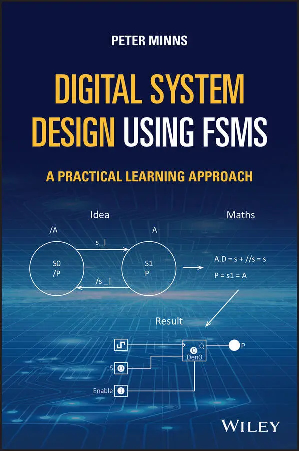
Peter D. Minns - Digital System Design using FSMs
Здесь есть возможность читать онлайн «Peter D. Minns - Digital System Design using FSMs» — ознакомительный отрывок электронной книги совершенно бесплатно, а после прочтения отрывка купить полную версию. В некоторых случаях можно слушать аудио, скачать через торрент в формате fb2 и присутствует краткое содержание. Жанр: unrecognised, на английском языке. Описание произведения, (предисловие) а так же отзывы посетителей доступны на портале библиотеки ЛибКат.
- Название:Digital System Design using FSMs
- Автор:
- Жанр:
- Год:неизвестен
- ISBN:нет данных
- Рейтинг книги:5 / 5. Голосов: 1
-
Избранное:Добавить в избранное
- Отзывы:
-
Ваша оценка:
Digital System Design using FSMs: краткое содержание, описание и аннотация
Предлагаем к чтению аннотацию, описание, краткое содержание или предисловие (зависит от того, что написал сам автор книги «Digital System Design using FSMs»). Если вы не нашли необходимую информацию о книге — напишите в комментариях, мы постараемся отыскать её.
Digital System Design using FSMs — читать онлайн ознакомительный отрывок
Ниже представлен текст книги, разбитый по страницам. Система сохранения места последней прочитанной страницы, позволяет с удобством читать онлайн бесплатно книгу «Digital System Design using FSMs», без необходимости каждый раз заново искать на чём Вы остановились. Поставьте закладку, и сможете в любой момент перейти на страницу, на которой закончили чтение.
Интервал:
Закладка:
Therefore, when the FSM enters state s1, the P output will be equal to logic 0 since /clk = 0 when the clock ‘clk’ is logic 1.
The clock will be logic 1 when the FSM enters state 1 (0 to 1 transition) the clock clk will then go to logic 0 (whilst still in state s1), and P will go to logic 1, then, when the clock clk goes back to logic 1 the FSM will move to state s2 and the flip‐flop outputs will no longer be A/B so the P output will not go high again. Therefore, the P output will only be logic 1 for a single clock clk pulse in state s1 when clk = 0 at the end of the state s1.
Figure 1.18illustrates this more clearly.
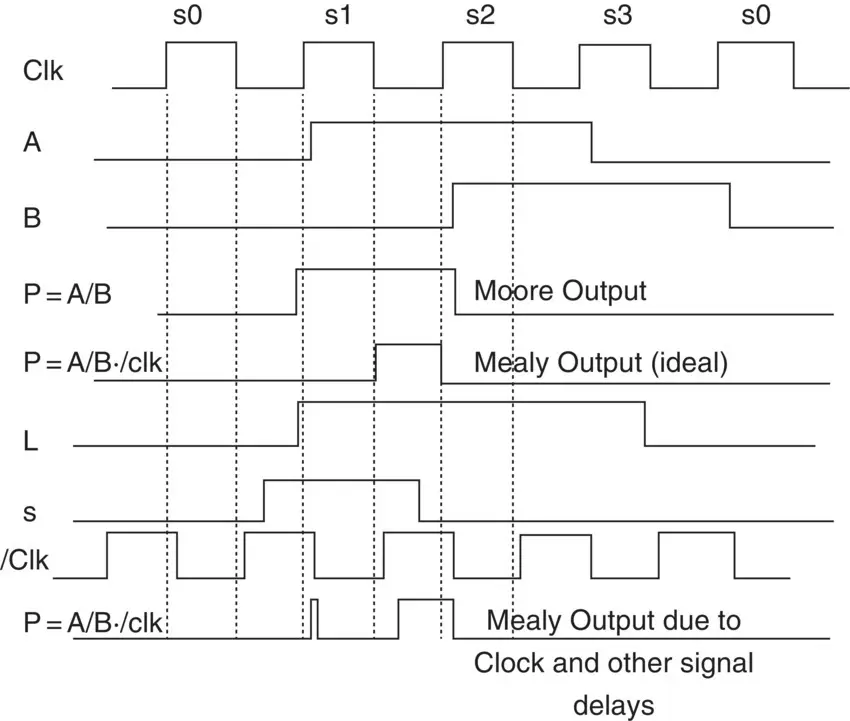
Figure 1.18 Timing diagram showing Moore and Mealy outputs.
The waveforms show both versions of P . As you can see, the Moore version raises P for the whole duration that the FSM is in state s1, whilst the Mealy version raises P for the time that the clock is low during state s1. Note in Figure 1.18 P = A/B·/Clk is not the same as P = A/B·clk.
Note the narrow pulse in the P Mealy signal during the second clk pulse. This is a glitch caused by signal delays in the A and clk signal lines. (See Chapter 4for more on this, but for now just accept it.)
There is quite a lot going on here so you might want to re‐read this frame again to fully understand it. We will be looking at the idea of using more Mealy outputs later on in this book.
It is possible to design state diagrams without Mealy outputs, using only Moore outputs. However, sometimes it is possible to reduce the size of a state diagram (less number of states) by using Mealy outputs. Examples are shown later.
Now for something a bit different.
Try producing a state diagram for an FSM that will produce a 101 pattern in response to an s input going high. Signal s must be returned low before another 101 pattern can be produced. In this example you are trying to use each state to produce the 101 pattern.
When you have attempted this task, turn to Frame 1.17 .
Frame 1.17
The solution to this problem is to use the basic arrangement of the single‐pulse state diagram and insert more states to generate the required 101 pattern ( Figure 1.19).
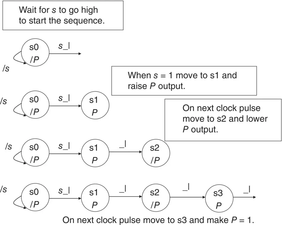
Figure 1.19 Development of a 101 pattern generator sequence.
It will develop state by state so you can see how it is done.
Note that we must leave state s3 on a clock pulse so that P = 1 for the duration of a single clock pulse only.
The final state required is to monitor for the input s = 0 condition.
This state should return the FSM back to state s0.
1 Complete the FSM state diagram then turn to Frame 1.18.
Frame 1.18
The completed state diagram is shown in Figure 1.20.
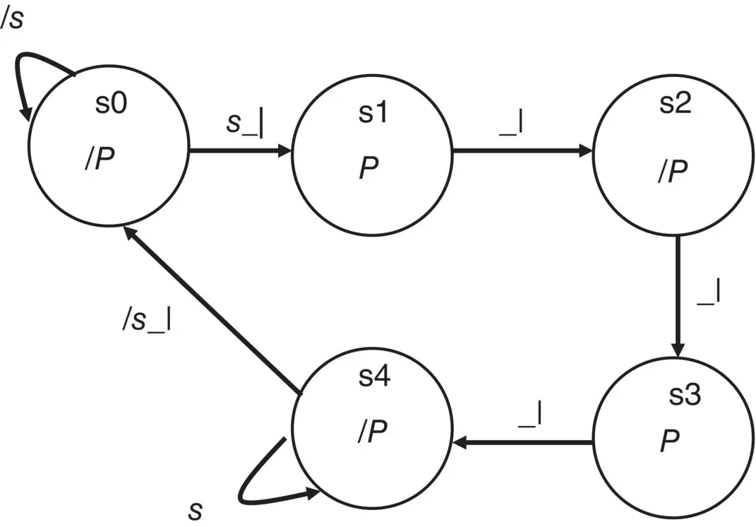
Figure 1.20 Complete state diagram for the 101 pattern generator.
The Boolean equation for P in this diagram is P = s1 + s3. However, we could make the P output a Mealy output that is only equal to 1 when in states s1 and s3, and only if the clock pulse is equal to 1.
Then, P = s1·clk + s3·clk since P must be high in both states s1 and s3, but only when the clock input is high.
Try writing an account of how this FSM works in your own words. If you get stuck, just re‐read Frames 1.16 and 1.17 again to refresh your memory.
Now try modifying the state diagram to make it produce a 101 sequence of clock pulses (in the same manner as shown in Frames 1.17 and 1.18 ).
Also, arrange for the P output pulse in state s3 to be conditional on a new input called x. If x = 0, the FSM should produce the output sequence 100 at P. If x = 1, the output sequence at P should be 101.
The reader may have noticed that the state diagram does not need to use slings. This is because slings are not really necessary with modern state diagrams. In fact, they are really only included for cosmetic reasons, to improve the readability of the design. From now on, only use slings where they improve the readability of the state diagram.
1 When you have done this, draw your state diagram and then turn to Frame 1.19.
Frame 1.19
Modify the state diagram to make it produce a 101 sequence of clock pulses (in the same manner as shown in Frames 1.15 and 1.16 . Also, arrange for the P output pulse in state s3 to be conditional on a new input called x. If x = 0, the FSM should produce the output sequence 100 at P. If x = 1, the output sequence at P should be 101.
The modified state diagram is shown in Figure 1.21.
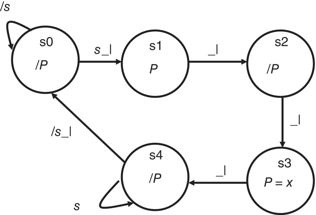
Figure 1.21 Modified state diagram with output P as a Mealy output.
In Figure 1.21, the clock is used as a qualifier in states s1 and s3 so that the output P is only logic 1 in these two states. However, state s3 has an additional qualifier x , so in s3 P = 1 only when in s3 and then only if input signal x is true in s3.
Then in state s3, the output P will only obtain a clock pulse if the x input happens to be logic 1.
You can see that if x = 0 then, when the input s is raised to logic 1, the FSM will produce the sequence 100 at output P . Therefore, P = s1 + s3· x . If x = 1 then, when s is raised to logic 1, the FSM will produce a 101 sequence at the output P .
This FSM is an example of a Mealy FSM since the output P is a function of both the state and the inputs clock and x , i.e. both clock and x are fed forward to the output decoding logic.
The reader could easily modify the FSM so that the 100 sequence at P was produced if x = 1, and the 101 sequence produced if x = 0. Therefore, now:
Produce the Boolean equation for P in state s3 that would satisfy this requirement.
Then assign a unit distance code to the state diagram; see Frames 1.12and 1.13.
Finally, when you have done that, try producing a timing diagram of the modified FSM.
When you’ve finished, turn to Frame 1.20 .
Frame 1.20
Produce the Boolean equation for P in state s3 that would satisfy this requirement.
The Boolean equation for P which will produce a 101 sequence when x = 0 is:
P = s3·/ x .
Note you do not need to indicate the clk, as it is assumed. Also note that in this case qualifying with NOT x (/ x ), rather than with x , as in Figure 1.22.
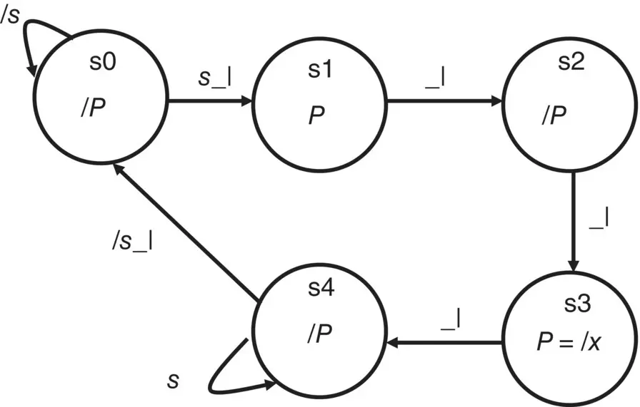
Figure 1.22 State diagram with Mealy P output in s3.
Читать дальшеИнтервал:
Закладка:
Похожие книги на «Digital System Design using FSMs»
Представляем Вашему вниманию похожие книги на «Digital System Design using FSMs» списком для выбора. Мы отобрали схожую по названию и смыслу литературу в надежде предоставить читателям больше вариантов отыскать новые, интересные, ещё непрочитанные произведения.


Обсуждение, отзывы о книге «Digital System Design using FSMs» и просто собственные мнения читателей. Оставьте ваши комментарии, напишите, что Вы думаете о произведении, его смысле или главных героях. Укажите что конкретно понравилось, а что нет, и почему Вы так считаете.