Peter D. Minns - Digital System Design using FSMs
Здесь есть возможность читать онлайн «Peter D. Minns - Digital System Design using FSMs» — ознакомительный отрывок электронной книги совершенно бесплатно, а после прочтения отрывка купить полную версию. В некоторых случаях можно слушать аудио, скачать через торрент в формате fb2 и присутствует краткое содержание. Жанр: unrecognised, на английском языке. Описание произведения, (предисловие) а так же отзывы посетителей доступны на портале библиотеки ЛибКат.

- Название:Digital System Design using FSMs
- Автор:
- Жанр:
- Год:неизвестен
- ISBN:нет данных
- Рейтинг книги:5 / 5. Голосов: 1
-
Избранное:Добавить в избранное
- Отзывы:
-
Ваша оценка:
Digital System Design using FSMs: краткое содержание, описание и аннотация
Предлагаем к чтению аннотацию, описание, краткое содержание или предисловие (зависит от того, что написал сам автор книги «Digital System Design using FSMs»). Если вы не нашли необходимую информацию о книге — напишите в комментариях, мы постараемся отыскать её.
Digital System Design using FSMs — читать онлайн ознакомительный отрывок
Ниже представлен текст книги, разбитый по страницам. Система сохранения места последней прочитанной страницы, позволяет с удобством читать онлайн бесплатно книгу «Digital System Design using FSMs», без необходимости каждый раз заново искать на чём Вы остановились. Поставьте закладку, и сможете в любой момент перейти на страницу, на которой закончили чтение.
Интервал:
Закладка:
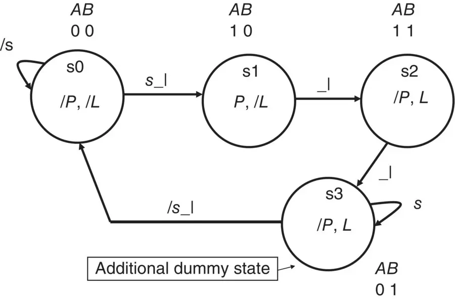
Figure 1.13 State diagram for single‐pulse generator with memory and dummy state.
Note that the added state has the unique name of s3 and the unique flip‐flop assignment of A = 0 and B = 1.
Also note that s2 uses the A and B values of A = 1 and B = 1. This provides the required unit distance coding.It also has the output P = 0, as it would in state s0 (the state it is going to go to when s = 0).
In this design the addition of the extra state has not added any more flip‐flops to the design since two flip‐flops can have a maximum of 2 2= 4 states (remember Frames 1.2and 1.3).
The addition of this extra state is usually called a dummy state.
Look carefully at the state diagram in Frame 1.13and satisfy yourself that the state diagram is doing the same thing as the one in Frame 1.11. If you cannot see this, consider reading Frames 1.11– 1.13again.
Now let us add an additional input called r to our state diagram.
Input r is to be added so that if r = 1 the FSM will continue to pulse output P (on and off) until r is made 0. At this point the FSM will return to state s0 but only if input s = 0.
Draw the block diagram for the FSM.
Draw the state diagram for this modified FSM.
Take your time and think about what you are doing.
Turn to Frame 1.14 when you have completed this task.
Frame 1.14
The block diagram in Figure 1.14is changing the behaviour of the state diagram.
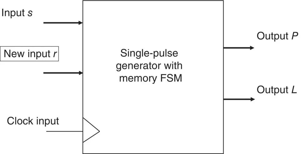
Figure 1.14 Block diagram for the FSM.
The state diagram is shown in Figure 1.15.
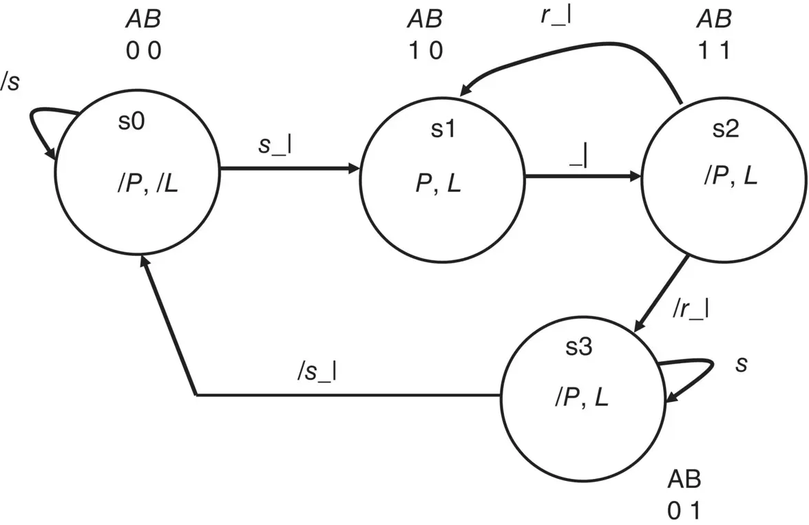
Figure 1.15 State diagram of single‐pulse generator with a multipulse feature.
The new state diagram is essentially the same as that in Frame 1.13except that now if r = 1 the state diagram sequence (with s = 1) becomes s0 → s1 → s2 → s1 → s2, and so on.
However, if s = 1 and r = 0 the sequence will be s0 → s1 → s2 → s3, which then stops until s = 0 then goes to s0.
From this you should understand that if we make r = 0 before we make s = 1 the state diagram will follow a single pulse on output P .
The Boolean equation for L can be active high or active low.
As active high, we look for states when the value of L is 1.

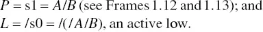
The Boolean equation for P was P = s1 = A / B (see Frame 1.12).
The Boolean equation for L = s1 + s2 + s3 = A + B since only in states s1, s2 and s3 is the output L = 1.
Note that an alternative equation for L could be the inverseequation for L , otherwise known as ‘active low’. Here we look for the states that make L = 0.

In practice there is a tendency to show this active low output as:
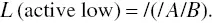
Note that to obtain the L = 0 the reader needs to invert s0 (/s0). This idea will be used later.
This is less complex so it may be used.
The latter equation is in terms of NOT L . This means that when in state s1, s2, or s3, L will be logic 1. Only when the FSM is NOT in any of these states will L = 0.
So in summary:
Input r is used with a two‐way branch from state s2.
If r = 0 there is no change in the operation of the FSM (single pulse from P).
However, if r = 1 the FSM will keep looping between s1 and s2 so as to keep turning the output P on and off, in effect using input r to change the operation of the FSM.
This shows how easily it is to change the behaviour of the FSM (in this case).
Note that this change was done in the state diagram then transferred to the actual FSM.
Please turn to Frame 1.15.
Frame 1.15
In the previous frames we have considered the flip‐flop output patterns. These are often referred to as the secondary state variables (SSVs)( Figure 1.16).
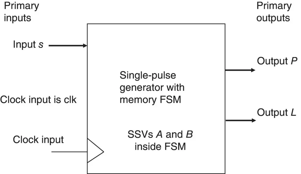
Figure 1.16 Block diagram showing secondary state variables in the FSM.
They are called ‘secondary state variables’ because they are (from the FSM architecture viewpoint) internal to the FSM (i.e. secondary not primary). If we consider the outside world inputs and outputs as being primary then it seems sensible to call the flip‐flop outputs SSVs (and state variables because they define the states of the state machine).
Moore and Mealy state diagram
The outputs in our FSM are seen to be dependent upon the SSVs or flip‐flops internal to the FSM. If you look back to Frame 1.5you will see that Moore FSM outputs are dependent upon the flip‐flop outputs only. The output decoding logic in our P pulse example is:
That is it consists of an AND gate and a NAND gate. This means that a single P pulse is a Moore FSM.
How could we make our single‐pulse design into a Mealy FSM?
One way would be to make the output P depend on the FSM being in state s1 ( A / B ), but we could say that the output was to be the width of a single logic 0 of the clock pulse.
How would we modify our state diagram to do this?
Try doing this, and then turn to Frame 1.16 to find out if you got it right.
Frame 1.16
The modified state diagram is shown in Figure 1.17(the r signal here has been dropped so we are back to a simple one‐pulse FSM). Also, /clk is clk inverted.
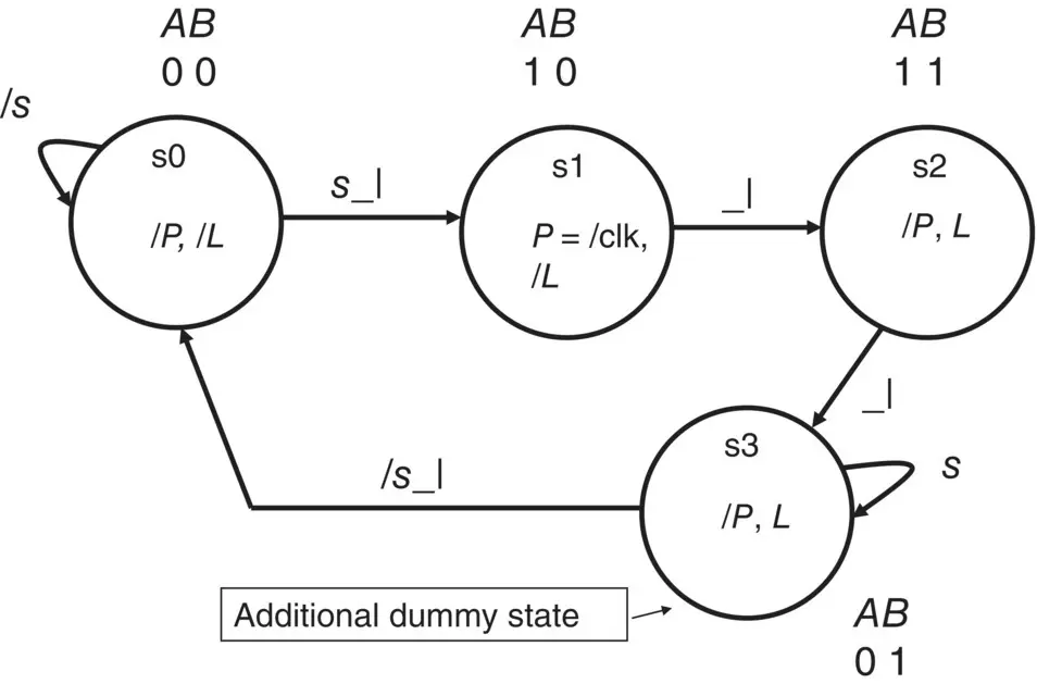
Figure 1.17 State diagram with Mealy output P .
Notice that now the output P is only equal to logic 1 when:
FSM is in state s1 where flip‐flop outputs are A = 1 and B = 0.
The clock signal is logic 0, as indicated by P = /clk.
Читать дальшеИнтервал:
Закладка:
Похожие книги на «Digital System Design using FSMs»
Представляем Вашему вниманию похожие книги на «Digital System Design using FSMs» списком для выбора. Мы отобрали схожую по названию и смыслу литературу в надежде предоставить читателям больше вариантов отыскать новые, интересные, ещё непрочитанные произведения.


Обсуждение, отзывы о книге «Digital System Design using FSMs» и просто собственные мнения читателей. Оставьте ваши комментарии, напишите, что Вы думаете о произведении, его смысле или главных героях. Укажите что конкретно понравилось, а что нет, и почему Вы так считаете.