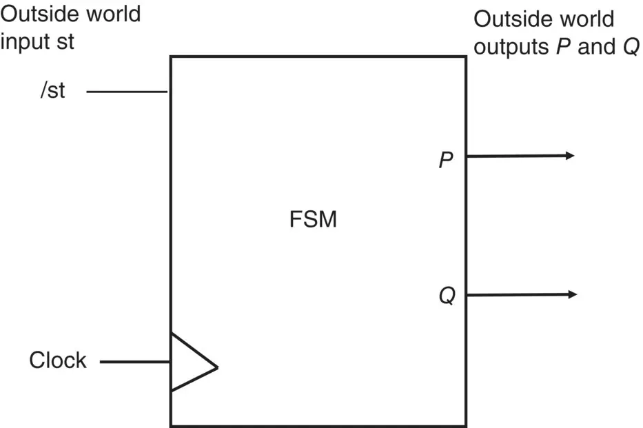
Figure 1.10 The block diagram for the state diagram shown in Figure 1.9.
Sometimes we show a negating circle to imply that the input is actually inverted (see later).
It is easily obtained from the state diagram since inputs lie along transitional lines and outputs lie inside (or alongside) the state circle. The input st would normally have a negating circleto show it is an active lowinput. This is common practice.
You may remember that in Frame 1.2we said that each state had to have a unique state number and that a number of flip‐flops were needed to perform this task. These flip‐flops are part of the internal design of the FSM and are used to produce an internal count sequence; they are essentially acting like a synchronous counter, but one that is controlled by the outside world inputs. The internal count sequence produced by the flip‐flops is used to control the outside world decoder so that outputs can be turned on and off as the FSM moves between states.
In Frames 1.4and 1.5we saw the architecture for the Mealy and Moore FSM. In both cases, the memory elements shown are the flip‐flops discussed in the previous paragraph. We look at how the internal flip‐flops are coded in a later chapter.
At this stage it is perhaps worth looking at a simple FSM design in detail. We can then bring together all the ideas discussed so far, as well as introducing a few new ones. Try answering the following questions before moving on:
1 A Mealy FSM differs from a Moore FSM in? (See Frames 1.4and 1.5.)
2 The circles in a state diagram are used to? (See Frames 1.8and 1.9.)
3 Outside world inputs are shown in a state diagram where? (See Frames 1.8and 1.9.)
4 Outside world outputs are shown where? (See Frame 1.9.)
5 The internal flip‐flops in an FSM are used to do what? (See Frame 1.10.)
Please turn to Frame 1.11 .
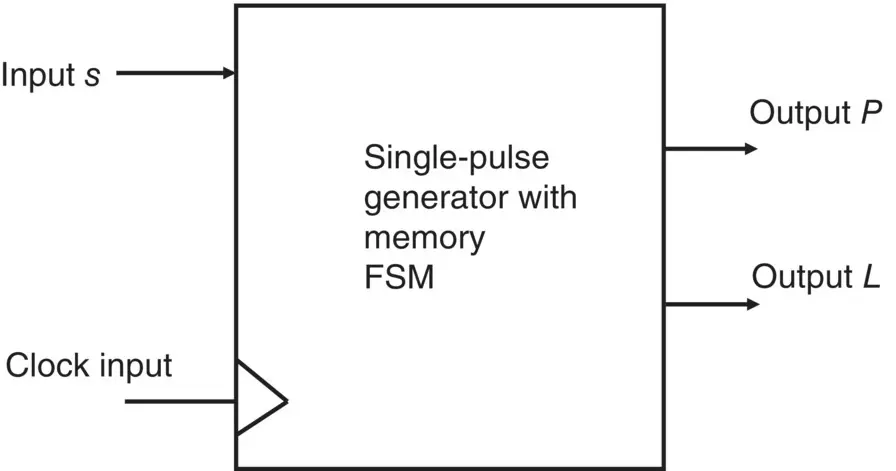
Figure 1.11shows an example of a single‐pule circuit FSM.
The idea here is to develop a circuit based on the FSM that will produce a single output pulse at its output P whenever its input s is taken to logic 1. The FSM is to be clock driven so it also has an input clock. An additional output L is used to indicate that a P pulse has been produced so the user can see effect of ‘fast’ pulses.
The block diagram of this circuit is shown in Figure 1.11.

Figure 1.11 Block diagram of single pulse with memory FSM.
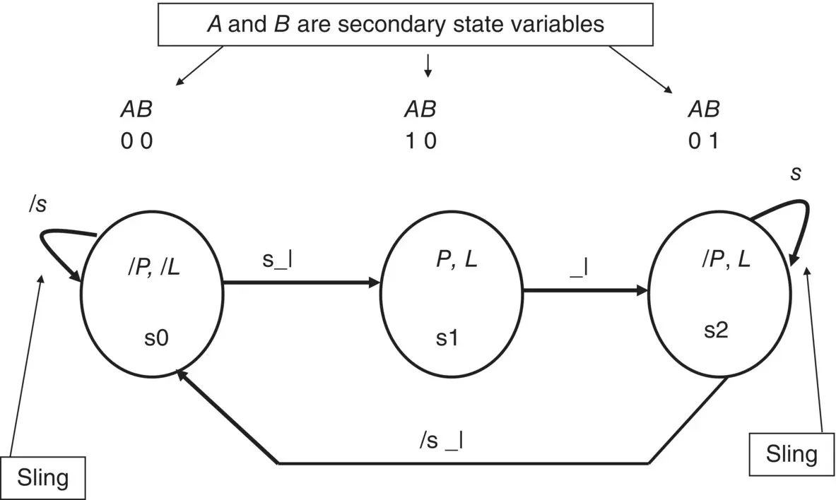
Figure 1.12shows a suitable state diagram.

Figure 1.12 State diagram for single pulse with memory FSM.
In this state diagram the sling(loop / s going to and from s0) indicates that while input s is logic 0 (/ s ) the FSM will remain in state s0 regardless of how many clock pulses are applied to the FSM. Only when input s goes to logic 1 will the FSM move from state s0 to s1, and then only when a clock pulse arrives. Once in state s1, the FSM will set its output P to logic 1, and on the next clock pulse the FSM will move from state s1 to s2.
The reason why the FSM will stay in state s1 for only one clock pulse is because in state s1 the transition from this state‐to‐state s2 occurs on a clock pulse only. Once the FSM arrives in state s2, it will remain there whilst input s = 1. As soon as input s goes to logic 0 (/ s ) the FSM will move back to state s0 on the next clock pulse.
Since the FSM remains in state s1 for only a single clock pulse, and since P = 1 only in state s1, the FSM will produce a single output pulse.
Note in the FSM state diagram that each state has a unique state identity: s0, s1, and s2.
Also note that each state has been allocated a unique combination of flip‐flop states, for example:
State s0 uses the flip‐flop combination A = 0 B = 0, e.g. both flip‐flops reset.
State s1 uses the flip‐flop combination A = 1 B = 0, e.g. flip‐flop A is set.
State s2 uses the flip‐flop combination A = 0 B = 1, e.g. flip‐flop A is reset, flip‐flop B is set.
Now move on to Frame 1.12 .
Let’s continue with the one‐pulse design.
The flip‐flop outputs are seen to define each state. If we could see nothing more than the A and B outputs of the two flip‐flops, we could tell what state the FSM was in by the output logic levels on each flip‐flop.
We could also tell in which state the output P was to be logic 1, i.e. in state s1 where the flip‐ flop output logic levels are A = 1 and B = 0.
Therefore, the output P = A / B . (Remember, AB is used to indicate the logical AND operation used in Boolean algebra.)
So we now see that the flip‐flops are used to provide a unique identity for each state.
We also see that, since each state can be defined in terms of the flip‐flop output states, the outside world outputs can also be defined in terms of the flip‐flop output states since the outside worlds output states themselves are a function of these states.
L is logic 1 in states s1 and s2 and is defined in terms of the flip‐flop outputs A / B + / AB .
Therefore, L = A / B + / AB = A / B + / AB . No Boolean reduction is possible in this case.
The allocation of unique values of flip‐flop outputs to each stateis rather an arbitrary process. In theory, we can use any values so long as each state has a unique combination. This means that we cannot have more than one state with the flip‐flop values of, say, A / B (i.e. both states cannot have the same value).
In practice it is common to assign flip‐flop values so that the transition between each state involves only one flip‐flop changing state. This is known as ‘following a unit distance pattern’: only one flip‐flop changes state.
The above example does not use a unit distance pattern since there are two flip‐flop changes between states s1 and s2. However, the reader will be going on to make use of the unit distance code idea.
The reader could also make the single‐pulse state diagram ( Figure 1.12) follow a unit distance patternby adding an extra state. This extra statecould be inserted between states s2 and s0, having the same output for P as state s0. In the state diagram the new state would also have the value of L , the same as that in state s2, since the reader does not want L to change until s goes to 0.
Try re‐drawing the state diagram with this additional state and assign a unit distance pattern to the flip‐flops.
When you have done this, go to Frame 1.13 .
A completed state diagram with unit distance patterns for flip‐flops is shown in Figure 1.13.
Читать дальше

