Thanks are also extended to: Dr C. Burch – Logisim, IET Digital Library, Oxford Publishing Limited, and Sage Publishing, USA for their various permissions, and these are referred to in the relevant sections of the book.
Any errors are, of course, entirely the responsibility of the author.
About the Companion Website
This book is accompanied by a companion website
www.wiley.com/go/minns/digitalsystemdesign 
This website includes:
An Index for Logisim Circuits
An Index for Verilog Listings
Guide to Supplementary Resources
Verilog HDL
Logisim Files

Guide to Supplementary Resources
The reader will be aware that this book is supported by working Logisim circuits and Verilog listings and these can be accessed via the Wiley website locator.
However in order to be able to access these Logisim and Verilog circuits/listings the reader needs to download two programs namely Logisim and SynaptiCAD Verilog HDL from the internet and install them on their computer (either PC or MAC) as explained in Appendix 2 of this book.
Each of the Logisim and Verilog HDL folders on the Wiley website has an individual index that shows the appropriate chapter/appendix reference locator to which they refer.
Once the appropriate software has been installed the reader will need to click onto either the .circ or .v files located in ‘Logisim Circuits for Web Folder’ or ‘Verilog Listings for Web Folder’ which they wish to access.
In both folders there is additional material and ideas that do not appear in this book but maybe of interest to the reader.
1 Introduction to Finite State Machines
This chapter (like all other chapters) is written in the form of a linear frame, programmed learning text. This is to help you learn the basic skills required to design clocked finite state machines (FMSs) so that you can develop your own designs based on traditional T flip‐flops and D flip‐flops. Later, other techniques will be introduced, such as ‘one hot’ and ‘asynchronous finite state machines’, but these will be developed along the same lines as the work covered in this chapter.
The text is organized into ‘frames’. Each frame follows on consecutively from the previous one, but at times you may be redirected to other frames, depending upon your response to the questions you are asked. Do not cheat, but follow the frames as indicated.
Bolddenotes questions for you to answerto check your understanding of the material, highlights important points, or indicates an aside when further ideas are presented.
Please read this chapter first, and attempt all the questions before moving on to the later chapters. Note that the book can be read as a textbook. The programmed aspect of the book makes it more suitable for individuals to read and learn in their own time.
Frame 1.1 What is a Finite State Machine?
A finite state machine (FSM) is a digital sequential circuit that can follow a number of predefined states under the control of one or more inputs. Each state is a stable entity that the machine can occupy. It can move from this state to another state under the control of an outside world input.

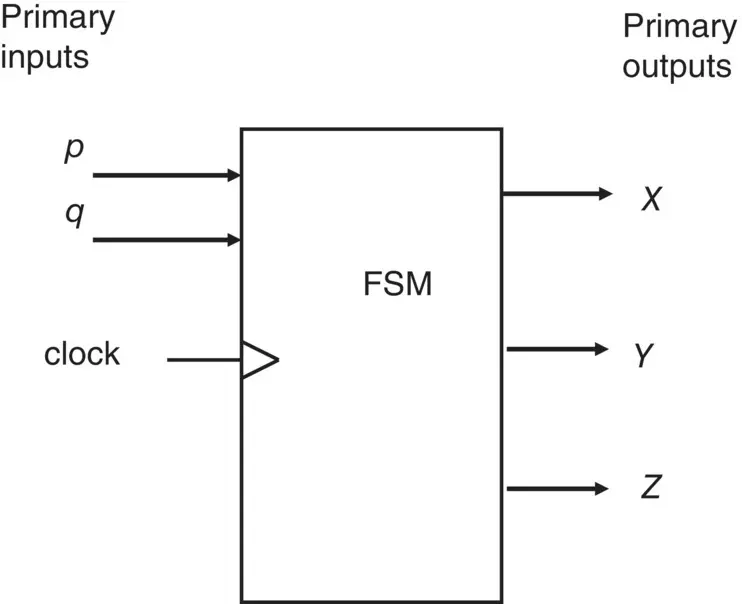
Figure 1.1 Block diagram of an FSM‐based application.
In Figure 1.1, we see an FSM with three outside world inputs ( p , q , and the clock) and three outside world outputs ( X , Y , and Z ). Note some FSMs have a clock input; those that don’t belong to a type of FSM called ‘asynchronous FSM’. However, this chapter deals with the more usual synchronous FSM, which dohave a clock input. Only Chapter 4and Chapter 6will look at asynchronous FSM.
Synchronous FSM can move between states only if a clock pulse occurs.
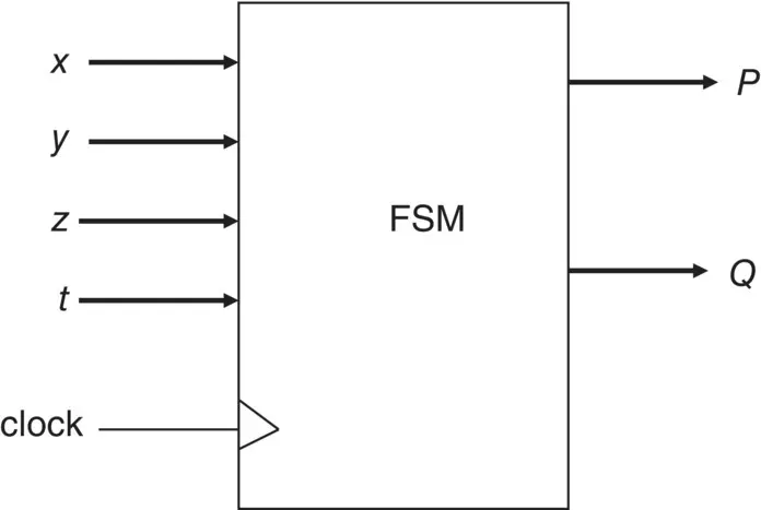
Task: Draw a block diagram for an FSM with five inputs (x, y, z, t, and a clock) and with two outputs (P and Q).
When you have done this, turn to Frame 1.2 .
The FSM with five inputs ( x , y , z , t , and a clock) and two outputs ( P and Q) is shown in Figure 1.2.
If you did not get this answer, go back and re‐read Frame 1.1. Don’t worry about using a mixture of both upper‐ and lower‐case letters here; the only thing that matters is that the same letters are used.
Each state of the FSM needs to be identifiable. This is achieved by using a number of internal flip‐flops within the FSM block. An FSM with four states would require two flip‐flops since two flip‐flops can store 2 2= 4 state numbers.

Figure 1.2 Block diagram with five inputs and two outputs.
Each state has a unique state number, and states are usually assigned numbers, such as s0 (state 0), s1, s2, and s3 (for a four‐state example).
As you can see, the rule here is 2 number of flip‐flops.
So an FSM with 13 states would require 2 4flip‐flops (i.e. 15 states of which 13 are used in the FSM and states 14 and 15 remain unused.
How many flip‐flops would be required for an FSM using 34 states?
What would the state numbers be for this FSM?
When you have answered these questions, turn to Frame 1.3 .
The answer to the previous question is:

In general: 2 4= 16 states, 2 5= 32 states, 2 6= 64 states, 2 7= 128 states, and so on.
What would the state number be for this FSM?

Answer:
The unused states would be s34 through to s63.
Note that the states run through from s0 to sn−1, for n states.
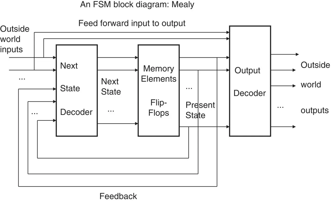
As well as containing flip‐flops to uniquely define the individual states of the FSM, there is also combinational logic, which defines the outside world outputs. In addition, the outside world inputs connect to combinational logic, which supplies the flip‐flops’ inputs.
Please turn to Frame 1.4 .
Figure 1.3illustrates the internal architecture for a Mealy FSM.

Figure 1.3 Block diagram of a Mealy state machine structure.
Читать дальше
