Ibrahim Dogan - Advanced PIC Microcontroller Projects in C
Здесь есть возможность читать онлайн «Ibrahim Dogan - Advanced PIC Microcontroller Projects in C» весь текст электронной книги совершенно бесплатно (целиком полную версию без сокращений). В некоторых случаях можно слушать аудио, скачать через торрент в формате fb2 и присутствует краткое содержание. Город: Burlington, Год выпуска: 2008, ISBN: 2008, Издательство: Elsevier Ltd, Жанр: Программирование, Компьютерное железо, на английском языке. Описание произведения, (предисловие) а так же отзывы посетителей доступны на портале библиотеки ЛибКат.
- Название:Advanced PIC Microcontroller Projects in C
- Автор:
- Издательство:Elsevier Ltd
- Жанр:
- Год:2008
- Город:Burlington
- ISBN:978-0-7506-8611-2
- Рейтинг книги:5 / 5. Голосов: 1
-
Избранное:Добавить в избранное
- Отзывы:
-
Ваша оценка:
Advanced PIC Microcontroller Projects in C: краткое содержание, описание и аннотация
Предлагаем к чтению аннотацию, описание, краткое содержание или предисловие (зависит от того, что написал сам автор книги «Advanced PIC Microcontroller Projects in C»). Если вы не нашли необходимую информацию о книге — напишите в комментариях, мы постараемся отыскать её.
• Features 20 complete, tried and test projects
• Includes a CD-ROM of all the programs, hex listings, diagrams, and data sheets
Advanced PIC Microcontroller Projects in C — читать онлайн бесплатно полную книгу (весь текст) целиком
Ниже представлен текст книги, разбитый по страницам. Система сохранения места последней прочитанной страницы, позволяет с удобством читать онлайн бесплатно книгу «Advanced PIC Microcontroller Projects in C», без необходимости каждый раз заново искать на чём Вы остановились. Поставьте закладку, и сможете в любой момент перейти на страницу, на которой закончили чтение.
Интервал:
Закладка:
Table 2.9: PIC18F452 PORTD pin functions
| Pin | Description |
|---|---|
| RD0/PSP0 | |
| RD0 | Digital I/O |
| PSP0 | Parallel slave port bit 0 |
| RD1/PSP1 | |
| RD1 | Digital I/O |
| PSP1 | Parallel slave port bit 1 |
| RD2/PSP2 | |
| RD2 | Digital I/O |
| PSP2 | Parallel slave port bit 2 |
| RD3/PSP3 | |
| RD3 | Digital I/O |
| PSP3 | Parallel slave port bit 3 |
| RD4/PSP4 | |
| RD4 | Digital I/O |
| PSP4 | Parallel slave port bit 4 |
| RD5/PSP5 | |
| RD5 | Digital I/O |
| PSP5 | Parallel slave port bit 5 |
| RD6/PSP6 | |
| RD6 | Digital I/O |
| PSP6 | Parallel slave port bit 6 |
| RD7/PSP7 | |
| RD7 | Digital I/O |
| PSP7 | Parallel slave port bit 7 |
In the PIC18F452 microcontroller, PORTE is only 3 bits wide. As shown in Table 2.10, port pins are shared with analog inputs and with parallel slave port read/write control bits. On a power-on reset, PORTE pins are configured as analog inputs and register ADCON1 must be programmed to change these pins to digital I/O.
Table 2.10: PIC18F452 PORTE pin functions
| Pin | Description |
|---|---|
| RE0/RD/AN5 | |
| RE0 | Digital I/O |
| RD | Parallel slave port read control pin |
| AN5 | Analog input 5 |
| RE1/WR/AN6 | |
| RE1 | Digital I/O |
| WR | Parallel slave port write control pin |
| AN6 | Analog input 6 |
| RE2/CS/AN7 | |
| RE2 | Digital I/O |
| CS | Parallel slave port CS |
| AN7 | Analog input 7 |
2.1.9 Timers
The PIC18F452 microcontroller has four programmable timers which can be used in many tasks, such as generating timing signals, causing interrupts to be generated at specific time intervals, measuring frequency and time intervals, and so on.
This section introduces the timers available in the PIC18F452 microcontroller.
Timer 0 is similar to the PIC16 series Timer 0, except that it can operate either in 8-bit or in 16-bit mode. Timer 0 has the following basic features:
• 8-bit or 16-bit operation
• 8-bit programmable prescaler
• External or internal clock source
• Interrupt generation on overflow
Timer 0 control register is T0CON, shown in Figure 2.24. The lower 6 bits of this register have similar functions to the PIC16-series OPTION register. The top two bits are used to select the 8-bit or 16-bit mode of operation and to enable/disable the timer.
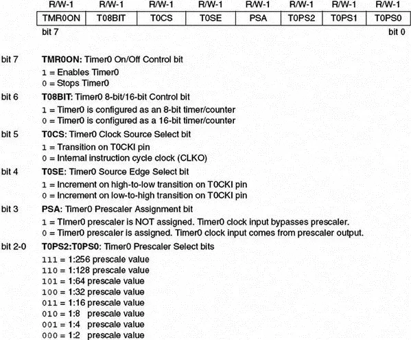
Figure 2.24: Timer 0 control register, T0CON
Timer 0 can be operated either as a timer or as a counter. Timer mode is selected by clearing the T0CS bit, and in this mode the clock to the timer is derived from F OSC/4. Counter mode is selected by setting the T0CS bit, and in this mode Timer 0 is incremented on the rising or falling edge of input RA4/T0CKI. Bit T0SE of T0CON selects the edge triggering mode.
An 8-bit prescaler can be used to change the timer clock rate by a factor of up to 256. The prescaler is selected by bits PSA and T0PS2:T0PS0 of register T0CON.
8-Bit Mode Figure 2.25 shows Timer 0 in 8-bit mode. The following operations are normally carried out in a timer application:
• Clear T0CS to select clock FOSC/4
• Use bits T0PS2:T0PS0 to select a suitable prescaler value
• Clear PSA to select the prescaler
• Load timer register TMR0L
• Optionally enable Timer 0 interrupts
• The timer counts up and an interrupt is generated when the timer value overflows from FFH to 00H in 8-bit mode (or from FFFFH to 0000H in 16-bit mode)
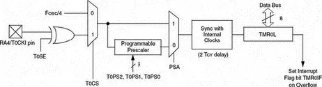
Figure 2.25: Timer 0 in 8-bit mode
By loading a value into the TMR0 register we can control the count until an overflow occurs. The formula that follows can be used to calculate the time it will take for the timer to overflow (or to generate an interrupt) given the oscillator period, the value loaded into the timer, and the prescaler value:
Overflow time = 4 × T OSC × Prescaler × (256–TMR0) (2.1)
where
Overflow time is in ms
T OSCis the oscillator period in μs
Prescaler is the prescaler value
TMR0 is the value loaded into TMR0 register
For example, assume that we are using a 4MHz crystal, and the prescaler is chosen as 1:8 by setting bits PS2:PS0 to 010. Also assume that the value loaded into the timer register TMR0 is decimal 100. The overflow time is then given by:
4MHZ clock has a period; T = 1/f = 0.25 μs
using the above formula
Overflow time = 4 × 0.25 × 8 × (256 – 100) = 1248 μs
Thus, the timer will overflow after 1.248 msec, and a timer interrupt will be generated if the timer interrupt and global interrupts are enabled.
What we normally want is to know what value to load into the TMR0 register for a required overflow time. This can be calculated by modifying Equation (2.1) as follows:
TMR0 = 256 – (Overflow time)/(4 × T OSC × Prescaler) (2.2)
For example, suppose we want an interrupt to be generated after 500ms and the clock and the prescaler values are as before. The value to be loaded into the TMR0 register can be calculated using Equation (2.2) as follows:
TMR0 = 256 – 500/(4 × 0.25 × 8) = 193.5
The closest number we can load into TMR0 register is 193.
16-Bit Mode The Timer 0 in 16-bit mode is shown in Figure 2.26. Here, two timer registers named TMR0L and TMR0 are used to store the 16-bit timer value. The low byte TMR0L is directly loadable from the data bus. The high byte TMR0 can be loaded through a buffer called TMR0H. During a read of TMR0L, the high byte of the timer (TMR0) is also loaded into TMR0H, and thus all 16 bits of the timer value can be read. To read the 16-bit timer value, first we have to read TMR0L, and then read TMR0H in a later instruction. Similarly, during a write to TMR0L, the high byte of the timer is also updated with the contents of TMR0H, allowing all 16 bits to be written to the timer. Thus, to write to the timer the program should first write the required high byte to TMR0H. When the low byte is written to TMR0L, then the value stored in TMR0H is automatically transferred to TMR0, thus causing all 16 bits to be written to the timer.
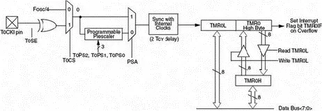
Figure 2.26: Timer 0 in 16-bit mode
PIC18F452 Timer 1 is a 16-bit timer controlled by register T1CON, as shown in Figure 2.27. Figure 2.28 shows the internal structure of Timer 1.
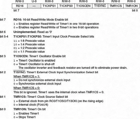
Figure 2.27: Timer 1 control register, T1CON
Читать дальшеИнтервал:
Закладка:
Похожие книги на «Advanced PIC Microcontroller Projects in C»
Представляем Вашему вниманию похожие книги на «Advanced PIC Microcontroller Projects in C» списком для выбора. Мы отобрали схожую по названию и смыслу литературу в надежде предоставить читателям больше вариантов отыскать новые, интересные, ещё непрочитанные произведения.


Обсуждение, отзывы о книге «Advanced PIC Microcontroller Projects in C» и просто собственные мнения читателей. Оставьте ваши комментарии, напишите, что Вы думаете о произведении, его смысле или главных героях. Укажите что конкретно понравилось, а что нет, и почему Вы так считаете.