Ibrahim Dogan - Advanced PIC Microcontroller Projects in C
Здесь есть возможность читать онлайн «Ibrahim Dogan - Advanced PIC Microcontroller Projects in C» весь текст электронной книги совершенно бесплатно (целиком полную версию без сокращений). В некоторых случаях можно слушать аудио, скачать через торрент в формате fb2 и присутствует краткое содержание. Город: Burlington, Год выпуска: 2008, ISBN: 2008, Издательство: Elsevier Ltd, Жанр: Программирование, Компьютерное железо, на английском языке. Описание произведения, (предисловие) а так же отзывы посетителей доступны на портале библиотеки ЛибКат.
- Название:Advanced PIC Microcontroller Projects in C
- Автор:
- Издательство:Elsevier Ltd
- Жанр:
- Год:2008
- Город:Burlington
- ISBN:978-0-7506-8611-2
- Рейтинг книги:5 / 5. Голосов: 1
-
Избранное:Добавить в избранное
- Отзывы:
-
Ваша оценка:
Advanced PIC Microcontroller Projects in C: краткое содержание, описание и аннотация
Предлагаем к чтению аннотацию, описание, краткое содержание или предисловие (зависит от того, что написал сам автор книги «Advanced PIC Microcontroller Projects in C»). Если вы не нашли необходимую информацию о книге — напишите в комментариях, мы постараемся отыскать её.
• Features 20 complete, tried and test projects
• Includes a CD-ROM of all the programs, hex listings, diagrams, and data sheets
Advanced PIC Microcontroller Projects in C — читать онлайн бесплатно полную книгу (весь текст) целиком
Ниже представлен текст книги, разбитый по страницам. Система сохранения места последней прочитанной страницы, позволяет с удобством читать онлайн бесплатно книгу «Advanced PIC Microcontroller Projects in C», без необходимости каждый раз заново искать на чём Вы остановились. Поставьте закладку, и сможете в любой момент перейти на страницу, на которой закончили чтение.
Интервал:
Закладка:
Table 2.3: PIC18F452 configuration register descriptions
| Configuration bits | Description |
|---|---|
| OSCSEN | Clock source switching enable |
| FOSC2:FOSC0 | Oscillator modes |
| BORV1:BORV0 | Brown-out reset voltage |
| BOREN | Brown-out reset enable |
| PWRTEN | Power-up timer enable |
| WDTPS2:WDTPS0 | Watchdog timer postscale bits |
| WDTEN | Watchdog timer enable |
| CCP2MX | CCP2 multiplex |
| DEBUG | Debug enable |
| LVP | Low-voltage program enable |
| STVREN | Stack full/underflow reset enable |
| CP3:CP0 | Code protection |
| CPD | EEPROM code protection |
| CPB | Boot block code protection |
| WRT3:WRT0 | Program memory write protection |
| WRTD | EPROM write protection |
| WRTB | Boot block write protection |
| WRTC | Configuration register write protection |
| EBTR3:EBTR0 | Table read protection |
| EBTRB | Boot block table read protection |
| DEV2:DEV0 | Device ID bits (001 = 18F452) |
| REV4:REV0 | Revision ID bits |
| DEV10:DEV3 | Device ID bits |
The CONFIG1H configuration register is at address 300001H and is used to select the microcontroller clock sources. The bit patterns are shown in Figure 2.6.
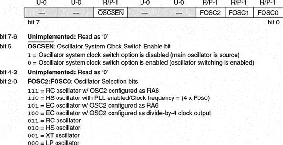
Figure 2.6: CONFIG1H register bits
The CONFIG2L configuration register is at address 300002H and is used to select the brown-out voltage bits. The bit patterns are shown in Figure 2.7.
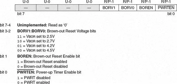
Figure 2.7: CONFIG2L register bits
The CONFIG2H configuration register is at address 300003H and is used to select the watchdog operations. The bit patterns are shown in Figure 2.8.
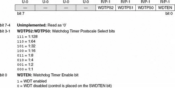
Figure 2.8: CONFIG2H register bits
2.1.4 The Power Supply
The power supply requirements of the PIC18F452 microcontroller are shown in Figure 2.9. As shown in Figure 2.10, PIC18F452 can operate with a supply voltage of 4.2V to 5.5V at the full speed of 40MHz. The lower power version, PIC18LF452, can operate from 2.0 to 5.5 volts. At lower voltages the maximum clock frequency is 4MHz, which rises to 40MHz at 4.2V. The RAM data retention voltage is specified as 1.5V and will be lost if the power supply voltage is lowered below this value. In practice, most microcontroller-based systems are operated with a single +5V supply derived from a suitable voltage regulator.
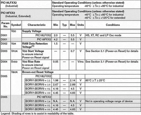
Figure 2.9: The PIC8F452 power supply parameters
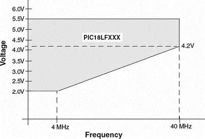
Figure 2.10: Operation of PIC18LF452 at different voltages
2.1.5 The Reset
The reset action puts the microcontroller into a known state. Resetting a PIC18F microcontroller starts execution of the program from address 0000H of the program memory. The microcontroller can be reset during one of the following operations:
• Power-on reset (POR)
• MCLR reset
• Watchdog timer (WDT) reset
• Brown-out reset (BOR)
• Reset instruction
• Stack full reset
• Stack underflow reset
Two types of resets are commonly used: power-on reset and external reset using the MCLR pin.
The power-on reset is generated automatically when power supply voltage is applied to the chip. The MCLR pin should be tied to the supply voltage directly or, preferably, through a 10K resistor. Figure 2.11 shows a typical reset circuit.
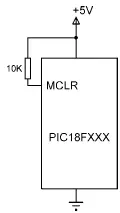
Figure 2.11: Typical reset circuit
For applications where the rise time of the voltage is slow, it is recommended to use a diode, a capacitor, and a series resistor as shown in Figure 2.12.
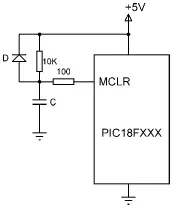
Figure 2.12: Reset circuit for slow-rising voltages
In some applications the microcontroller may have to be reset externally by pressing a button. Figure 2.13 shows the circuit that can be used to reset the microcontroller externally. Normally the MCLR input is at logic 1. When the RESET button is pressed, this pin goes to logic 0 and resets the microcontroller.
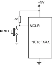
Figure 2.13: External reset circuit
2.1.6 The Clock Sources
The PIC18F452 microcontroller can be operated from an external crystal or ceramic resonator connected to the microcontroller’s OSC1 and OSC2 pins. In addition, an external resistor and capacitor, an external clock source, and in some models internal oscillators can be used to provide clock pulses to the microcontroller. There are eight clock sources on the PIC18F452 microcontroller, selected by the configuration register CONFIG1H. These are:
• Low-power crystal (LP)
• Crystal or ceramic resonator (XT)
• High-speed crystal or ceramic resonator (HS)
• High-speed crystal or ceramic resonator with PLL (HSPLL)
• External clock with F OSC/4on OSC2 (EC)
• External clock with I/O on OSC2 (port RA6) (ECIO)
• External resistor/capacitor with F OSC/4output on OSC2 (RC)
• External resistor/capacitor with I/O on OSC2 (port RA6) (RCIO)
The first several clock sources listed use an external crystal or ceramic resonator that is connected to the OSC1 and OSC2 pins. For applications where accuracy of timing is important, a crystal should be used. And if a crystal is used, a parallel resonant crystal must be chosen, since series resonant crystals do not oscillate when the system is first powered.
Figure 2.14 shows how a crystal is connected to the microcontroller. The capacitor values depend on the mode of the crystal and the selected frequency. Table 2.4 gives the recommended values. For example, for a 4MHz crystal frequency, use 15pF capacitors. Higher capacitance increases the oscillator stability but also increases the start-up time.
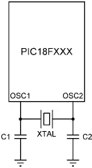
Figure 2.14: Using a crystal as the clock input
Table 2.4: Capacitor values
| Mode | Frequency | C1,C2 (pF) |
|---|---|---|
| LP | 32 KHz | 33 |
| 200 KHz | 15 | |
| XT | 200 KHz | 22–68 |
| 1.0 MHz | 15 | |
| 4.0 MHz | 15 | |
| HS | 4.0 MHz | 15 |
| 8.0 MHz | 15–33 | |
| 20.0 MHz | 15–33 | |
| 25.0 MHz | 15–33 |
Resonators should be used in low-cost applications where high accuracy in timing is not required. Figure 2.15 shows how a resonator is connected to the microcontroller.
Читать дальшеИнтервал:
Закладка:
Похожие книги на «Advanced PIC Microcontroller Projects in C»
Представляем Вашему вниманию похожие книги на «Advanced PIC Microcontroller Projects in C» списком для выбора. Мы отобрали схожую по названию и смыслу литературу в надежде предоставить читателям больше вариантов отыскать новые, интересные, ещё непрочитанные произведения.


Обсуждение, отзывы о книге «Advanced PIC Microcontroller Projects in C» и просто собственные мнения читателей. Оставьте ваши комментарии, напишите, что Вы думаете о произведении, его смысле или главных героях. Укажите что конкретно понравилось, а что нет, и почему Вы так считаете.