Ibrahim Dogan - Advanced PIC Microcontroller Projects in C
Здесь есть возможность читать онлайн «Ibrahim Dogan - Advanced PIC Microcontroller Projects in C» весь текст электронной книги совершенно бесплатно (целиком полную версию без сокращений). В некоторых случаях можно слушать аудио, скачать через торрент в формате fb2 и присутствует краткое содержание. Город: Burlington, Год выпуска: 2008, ISBN: 2008, Издательство: Elsevier Ltd, Жанр: Программирование, Компьютерное железо, на английском языке. Описание произведения, (предисловие) а так же отзывы посетителей доступны на портале библиотеки ЛибКат.
- Название:Advanced PIC Microcontroller Projects in C
- Автор:
- Издательство:Elsevier Ltd
- Жанр:
- Год:2008
- Город:Burlington
- ISBN:978-0-7506-8611-2
- Рейтинг книги:5 / 5. Голосов: 1
-
Избранное:Добавить в избранное
- Отзывы:
-
Ваша оценка:
Advanced PIC Microcontroller Projects in C: краткое содержание, описание и аннотация
Предлагаем к чтению аннотацию, описание, краткое содержание или предисловие (зависит от того, что написал сам автор книги «Advanced PIC Microcontroller Projects in C»). Если вы не нашли необходимую информацию о книге — напишите в комментариях, мы постараемся отыскать её.
• Features 20 complete, tried and test projects
• Includes a CD-ROM of all the programs, hex listings, diagrams, and data sheets
Advanced PIC Microcontroller Projects in C — читать онлайн бесплатно полную книгу (весь текст) целиком
Ниже представлен текст книги, разбитый по страницам. Система сохранения места последней прочитанной страницы, позволяет с удобством читать онлайн бесплатно книгу «Advanced PIC Microcontroller Projects in C», без необходимости каждый раз заново искать на чём Вы остановились. Поставьте закладку, и сможете в любой момент перейти на страницу, на которой закончили чтение.
Интервал:
Закладка:
| Pin | Description |
|---|---|
| RA0/AN0 | |
| RA0 | Digital I/O |
| AN0 | Analog input 0 |
| RA1/AN1 | |
| RA1 | Digital I/O |
| AN1 | Analog input 1 |
| RA2/AN2/VREF– | |
| RA2 | Digital I/O |
| AN2 | Analog input 2 |
| VREF– | A/D reference voltage (low) input |
| RA3/AN3/VREF+ | |
| RA3 | Digital I/O |
| AN3 | Analog input 3 |
| VREF+ | A/D reference voltage (high) input |
| RA4/T0CKI | |
| RA4 | Digital I/O |
| T0CKI | Timer 0 external clock input |
| RA5/AN4/SS/LVDIN | |
| RA5 | Digital I/O |
| AN4 | Analog input 4 |
| SS | SPI Slave Select input |
| RA6 | Digital I/O |
The architecture of PORTA is shown in Figure 2.22. There are three registers associated with PORTA:
• Port data register — PORTA
• Port direction register — TRISA
• Port latch register — LATA
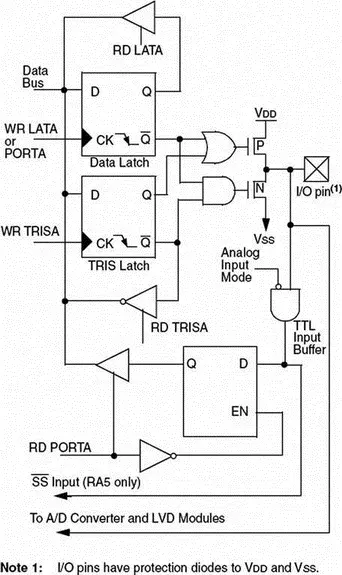
Figure 2.22: PIC18F452 PORTA RA0–RA3 and RA5 pins
PORTA is the name of the port data register. The TRISA register defines the direction of PORTA pins, where a logic 1 in a bit position defines the pin as an input pin, and a 0 in a bit position defines it as an output pin. LATA is the output latch register which shares the same data latch as PORTA. Writing to one is equivalent to writing to the other. But reading from LATA activates the buffer at the top of the diagram, and the value held in the PORTA/LATA data latch is transferred to the data bus independent of the state of the actual output pin of the microcontroller.
Bits 0 through 3 and 5 of PORTA are also used as analog inputs. After a device reset, these pins are programmed as analog inputs and RA4 and RA6 are configured as digital inputs. To program the analog inputs as digital I/O, the ADCON1 register (A/D register) must be programmed accordingly. Writing 7 to ADCON1 configures all PORTA pins as digital I/O.
The RA4 pin is multiplexed with the Timer 0 clock input (T0CKI). This is a Schmitt trigger input and an open drain output.
RA6 can be used as a general purpose I/O pin, as the OSC2 clock input, or as a clock output providing F OSC/4clock pulses.
In PIC18F452 microcontroller PORTB is an 8-bit bidirectional port shared with interrupt pins and serial device programming pins. Table 2.7 gives the PORTB bit functions.
Table 2.7: PIC18F452 PORTB pin functions
| Pin | Description |
|---|---|
| RB0/INT0 | |
| RB0 | Digital I/O |
| INT0 | External interrupt 0 |
| RB1/INT1 | |
| RB1 | Digital I/O |
| INT1 | External interrupt 1 |
| RB2/INT2 | |
| RB2 | Digital I/O |
| INT2 | External interrupt 2 |
| RB3/CCP2 | |
| RB3 | Digital I/O |
| CCP2 | Capture 2 input, compare 2, and PWM2 output |
| RB4 | Digital I/O, interrupt on change pin |
| RB5/PGM | |
| RB5 | Digital I/O, interrupt on change pin |
| PGM | Low-voltage ICSP programming pin |
| RB6/PGC | |
| RB6 | Digital I/O, interrupt on change pin |
| PGC | In-circuit debugger and ICSP programming pin |
| RB7/PGD | |
| RB7 | Digital I/O, interrupt on change pin |
| PGD | In-circuit debugger and ICSP programming pin |
PORTB is controlled by three registers:
• Port data register — PORTB
• Port direction register — TRISB
• Port latch register — LATB
The general operation of PORTB is similar to that of PORTA. Figure 2.23 shows the architecture of PORTB. Each port pin has a weak internal pull-up which can be enabled by clearing bit RBPU of register INTCON2. These pull-ups are disabled on a power-on reset and when the port pin is configured as an output. On a power-on reset, PORTB pins are configured as digital inputs. Internal pull-ups allow input devices such as switches to be connected to PORTB pins without the use of external pull-up resistors. This saves costs because the component count and wiring requirements are reduced.
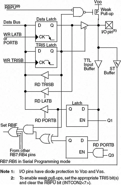
Figure 2.23: PIC18F452 PORTB RB4–RB7 pins
Port pins RB4–RB7 can be used as interrupt-on-change inputs, whereby a change on any of pins 4 through 7 causes an interrupt flag to be set. The interrupt enable and flag bits RBIE and RBIF are in register INTCON.
In addition to PORTA and PORTB, the PIC18F452 has 8-bit bidirectional ports PORTC and PORTD, and 3-bit PORTE. Each port has its own data register (e.g., PORTC), data direction register (e.g., TRISC), and data latch register (e.g., LATC). The general operation of these ports is similar to that of PORTA.2.1.
In the PIC18F452 microcontroller PORTC is multiplexed with several peripheral functions as shown in Table 2.8. On a power-on reset, PORTC pins are configured as digital inputs.
Table 2.8: PIC18F452 PORTC pin functions
| Pin | Description |
|---|---|
| RC0/T1OSO/T1CKI | |
| RC0 | Digital I/O |
| T1OSO | Timer 1 oscillator output |
| T1CKI | Timer 1/Timer 3 external clock input |
| RC1/T1OSI/CCP2 | |
| RC1 | Digital I/O |
| T1OSI | Timer 1 oscillator input |
| CCP2 | Capture 2 input, Compare 2 and PWM2 output |
| RC2/CCP1 | |
| RC2 | Digital I/O |
| CCP1 | Capture 1 input, Compare 1 and PWM1 output |
| RC3/SCK/SCL | |
| RC3 | Digital I/O |
| SCK | Synchronous serial clock input/output for SPI |
| SCL | Synchronous serial clock input/output for I²C |
| RC4/SDI/SDA | |
| RC4 | Digital I/O |
| SDI | SPI data in |
| SDA | I²C data I/O |
| RC5/SDO | |
| RC5 | Digital I/O |
| SDO | SPI data output |
| RC6/TX/CK | |
| RC6 | Digital I/O |
| TX | USART transmit pin |
| CK | USART synchronous clock pin |
| RC7/RX/DT | |
| RC7 | Digital I/O |
| RX | USART receive pin |
| DT | USART synchronous data pin |
In the PIC18F452 microcontroller, PORTD has Schmitt trigger input buffers. On a power-on reset, PORTD is configured as digital input. PORTD can be configured as an 8-bit parallel slave port (i.e., a microprocessor port) by setting bit 4 of the TRISE register. Table 2.9 shows functions of PORTD pins.
Читать дальшеИнтервал:
Закладка:
Похожие книги на «Advanced PIC Microcontroller Projects in C»
Представляем Вашему вниманию похожие книги на «Advanced PIC Microcontroller Projects in C» списком для выбора. Мы отобрали схожую по названию и смыслу литературу в надежде предоставить читателям больше вариантов отыскать новые, интересные, ещё непрочитанные произведения.


Обсуждение, отзывы о книге «Advanced PIC Microcontroller Projects in C» и просто собственные мнения читателей. Оставьте ваши комментарии, напишите, что Вы думаете о произведении, его смысле или главных героях. Укажите что конкретно понравилось, а что нет, и почему Вы так считаете.