Ibrahim Dogan - Advanced PIC Microcontroller Projects in C
Здесь есть возможность читать онлайн «Ibrahim Dogan - Advanced PIC Microcontroller Projects in C» весь текст электронной книги совершенно бесплатно (целиком полную версию без сокращений). В некоторых случаях можно слушать аудио, скачать через торрент в формате fb2 и присутствует краткое содержание. Город: Burlington, Год выпуска: 2008, ISBN: 2008, Издательство: Elsevier Ltd, Жанр: Программирование, Компьютерное железо, на английском языке. Описание произведения, (предисловие) а так же отзывы посетителей доступны на портале библиотеки ЛибКат.
- Название:Advanced PIC Microcontroller Projects in C
- Автор:
- Издательство:Elsevier Ltd
- Жанр:
- Год:2008
- Город:Burlington
- ISBN:978-0-7506-8611-2
- Рейтинг книги:5 / 5. Голосов: 1
-
Избранное:Добавить в избранное
- Отзывы:
-
Ваша оценка:
Advanced PIC Microcontroller Projects in C: краткое содержание, описание и аннотация
Предлагаем к чтению аннотацию, описание, краткое содержание или предисловие (зависит от того, что написал сам автор книги «Advanced PIC Microcontroller Projects in C»). Если вы не нашли необходимую информацию о книге — напишите в комментариях, мы постараемся отыскать её.
• Features 20 complete, tried and test projects
• Includes a CD-ROM of all the programs, hex listings, diagrams, and data sheets
Advanced PIC Microcontroller Projects in C — читать онлайн бесплатно полную книгу (весь текст) целиком
Ниже представлен текст книги, разбитый по страницам. Система сохранения места последней прочитанной страницы, позволяет с удобством читать онлайн бесплатно книгу «Advanced PIC Microcontroller Projects in C», без необходимости каждый раз заново искать на чём Вы остановились. Поставьте закладку, и сможете в любой момент перейти на страницу, на которой закончили чтение.
Интервал:
Закладка:
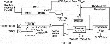
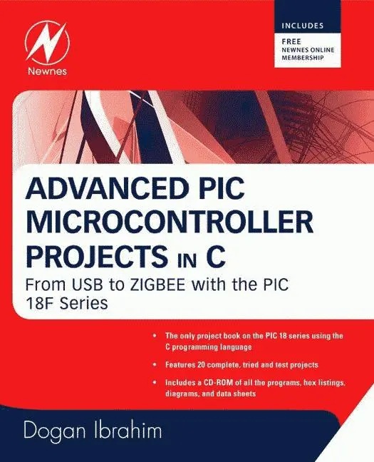
Figure 2.28: Internal structure of Timer 1
Timer 1 can be operated as either a timer or a counter. When bit TMR1CS of register T1CON is low, clock FOSC/4 is selected for the timer. When TMR1CS is high, the module operates as a counter clocked from input T1OSI. A crystal oscillator circuit, enabled from bit T1OSCEN of T1CON, is built between pins T1OSI and T1OSO where a crystal up to 200KHz can be connected between these pins. This oscillator is primarily intended for a 32KHz crystal operation in real-time clock applications. A prescaler is used in Timer 1 that can change the timing rate as a factor of 1, 2, 4, or 8.
Timer 1 can be configured so that read/write can be performed either in 16-bit mode or in two 8-bit modes. Bit RD16 of register T1CON controls the mode. When RD16 is low, timer read and write operations are performed as two 8-bit operations. When RD16 is high, the timer read and write operations are as in Timer 0 16-bit mode (i.e., a buffer is used between the timer register and the data bus) (see Figure 2.29).
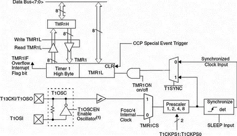
Figure 2.29: Timer 1 in 16-bit mode
If the Timer 1 interrupts are enabled, an interrupt will be generated when the timer value rolls over from FFFFH to 0000H.
Timer 2 is an 8-bit timer with the following features:
• 8-bit timer (TMR2)
• 8-bit period register (PR2)
• Programmable prescaler
• Programmable postscaler
• Interrupt when TM2 matches PR2
Timer 2 is controlled from register T2CON, as shown in Figure 2.30. Bits T2CKPS1:T2CKPS0 set the prescaler for a scaling of 1, 4, and 16. Bits TOUTPS3:TOUTPS0 set the postscaler for a scaling of 1:1 to 1:16. The timer can be turned on or off by setting or clearing bit TMR2ON.
Figure 2.30: Timer 2 control register, T2CON
The block diagram of Timer 2 is shown in Figure 2.31. Timer 2 can be used for the PWM mode of the CCP module. The output of Timer 2 can be software selected by the SSP module as a baud clock. Timer 2 increments from 00H until it matches PR2 and sets the interrupt flag. It then resets to 00H on the next cycle.
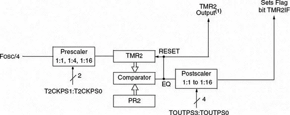
Figure 2.31: Timer 2 block diagram
The structure and operation of Timer 3 is the same as for Timer 1, having registers TMR3H and TMR3L. This timer is controlled from register T3CON as shown in Figure 2.32.
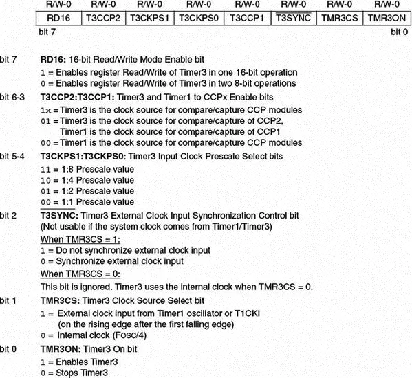
Figure 2.32: Timer 3 control register, T3CON
The block diagram of Timer 3 is shown in Figure 2.33.
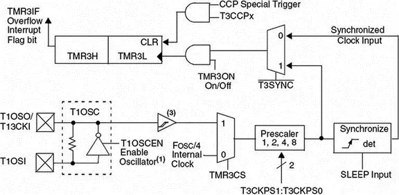
Figure 2.33: Block diagram of Timer 3
2.1.10 Capture/Compare/PWM Modules (CCP)
The PIC18F452 microcontroller has two capture/compare/PWM (CCP) modules, and they work with Timers 1, 2, and 3 to provide capture, compare, and pulse width modulation (PWM) operations. Each module has two 8-bit registers. Module 1 registers are CCPR1L and CCPR1H, and module 2 registers are CCPR2L and CCPR2H. Together, each register pair forms a 16-bit register and can be used to capture, compare, or generate waveforms with a specified duty cycle. Module 1 is controlled by register CCP1CON, and module 2 is controlled by CCP2CON. Figure 2.34 shows the bit allocations of the CCP control registers.
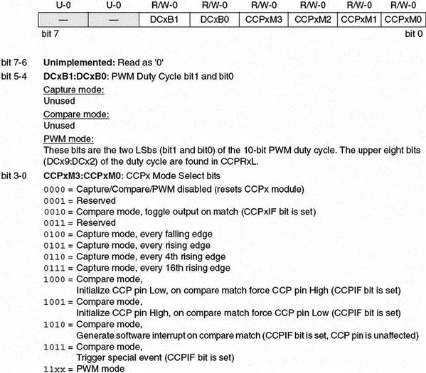
Figure 2.34: CCPxCON register bit allocations
In capture mode, the registers operate like a stopwatch. When an event occurs, the time of the event is recorded, although the clock continues running (a stopwatch, on the other hand, stops when the event time is recorded).
Figure 2.35 shows the capture mode of operation. Here, CCP1 will be considered, but the operation of CCP2 is identical with the register and port names changed accordingly. In this mode CCPR1H:CCPR1L captures the 16-bit value of the TMR1 or TMR3 registers when an event occurs on pin RC2/CCP1 (pin RC2/CCP1 must be configured as an input pin using TRISC). An external signal can be prescaled by 4 or 16. The event is selected by control bits CCP1M3:CCP1M0, and any of the following events can be selected:
• Every falling edge
• Every rising edge
• Every fourth rising edge
• Every sixteenth rising edge
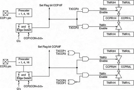
Figure 2.35: Capture mode of operation
If the capture interrupt is enabled, the occurrence of an event causes an interrupt to be generated in software. If another capture occurs before the value in register CCPR1 is read, the old captured value is overwritten by the new captured value.
Either Timer 1 or Timer 3 can be used in capture mode. They must be running in timer mode, or in synchronized counter mode, selected by register T3CON.
In compare mode, a digital comparator is used to compare the value of Timer 1 or Timer 3 to the value in a 16-bit register pair. When a match occurs, the output state of a pin is changed. Figure 2.36 shows the block diagram of compare mode in operation.
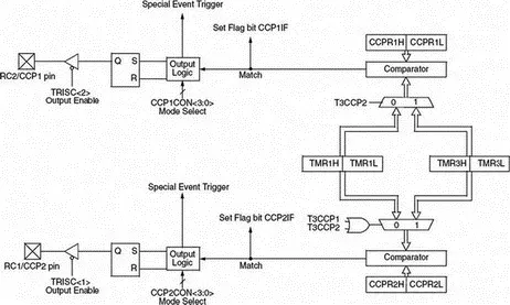
Figure 2.36: Compare mode of operation
Here only module CCP1 is considered, but the operation of module CCP2 is identical.
The value of the 16-bit register pair CCPR1H:CCPR1L is continuously compared against the Timer 1 or Timer 3 value. When a match occurs, the state of the RC2/CCP1 pin is changed depending on the programming of bits CCP1M2:CCP1M0 of register CCP1CON. The following changes can be programmed:
• Force RC2/CCP1 high
• Force RC2/CCP1 low
• Toggle RC2/CCP1 pin (low to high or high to low)
• Generate interrupt when a match occurs
• No change
Timer 1 or Timer 3 must be running in timer mode or in synchronized counter mode, selected by register T3CON.
The pulse width modulation (PWM) mode produces a PWM output at 10-bit resolution. A PWM output is basically a square waveform with a specified period and duty cycle. Figure 2.37 shows a typical PWM waveform.
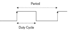
Figure 2.37: Typical PWM waveform
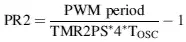
Figure 2.38 shows the PWM module block diagram. The module is controlled by Timer 2. The PWM period is given by:
PWM period = (PR2 + 1) * TMR2PS * 4 * T OSC (2.3)
or
 (2.4)
(2.4)
where
PR2 is the value loaded into Timer 2 register
Читать дальшеИнтервал:
Закладка:
Похожие книги на «Advanced PIC Microcontroller Projects in C»
Представляем Вашему вниманию похожие книги на «Advanced PIC Microcontroller Projects in C» списком для выбора. Мы отобрали схожую по названию и смыслу литературу в надежде предоставить читателям больше вариантов отыскать новые, интересные, ещё непрочитанные произведения.


Обсуждение, отзывы о книге «Advanced PIC Microcontroller Projects in C» и просто собственные мнения читателей. Оставьте ваши комментарии, напишите, что Вы думаете о произведении, его смысле или главных героях. Укажите что конкретно понравилось, а что нет, и почему Вы так считаете.