Ibrahim Dogan - Advanced PIC Microcontroller Projects in C
Здесь есть возможность читать онлайн «Ibrahim Dogan - Advanced PIC Microcontroller Projects in C» весь текст электронной книги совершенно бесплатно (целиком полную версию без сокращений). В некоторых случаях можно слушать аудио, скачать через торрент в формате fb2 и присутствует краткое содержание. Город: Burlington, Год выпуска: 2008, ISBN: 2008, Издательство: Elsevier Ltd, Жанр: Программирование, Компьютерное железо, на английском языке. Описание произведения, (предисловие) а так же отзывы посетителей доступны на портале библиотеки ЛибКат.
- Название:Advanced PIC Microcontroller Projects in C
- Автор:
- Издательство:Elsevier Ltd
- Жанр:
- Год:2008
- Город:Burlington
- ISBN:978-0-7506-8611-2
- Рейтинг книги:5 / 5. Голосов: 1
-
Избранное:Добавить в избранное
- Отзывы:
-
Ваша оценка:
Advanced PIC Microcontroller Projects in C: краткое содержание, описание и аннотация
Предлагаем к чтению аннотацию, описание, краткое содержание или предисловие (зависит от того, что написал сам автор книги «Advanced PIC Microcontroller Projects in C»). Если вы не нашли необходимую информацию о книге — напишите в комментариях, мы постараемся отыскать её.
• Features 20 complete, tried and test projects
• Includes a CD-ROM of all the programs, hex listings, diagrams, and data sheets
Advanced PIC Microcontroller Projects in C — читать онлайн бесплатно полную книгу (весь текст) целиком
Ниже представлен текст книги, разбитый по страницам. Система сохранения места последней прочитанной страницы, позволяет с удобством читать онлайн бесплатно книгу «Advanced PIC Microcontroller Projects in C», без необходимости каждый раз заново искать на чём Вы остановились. Поставьте закладку, и сможете в любой момент перейти на страницу, на которой закончили чтение.
Интервал:
Закладка:
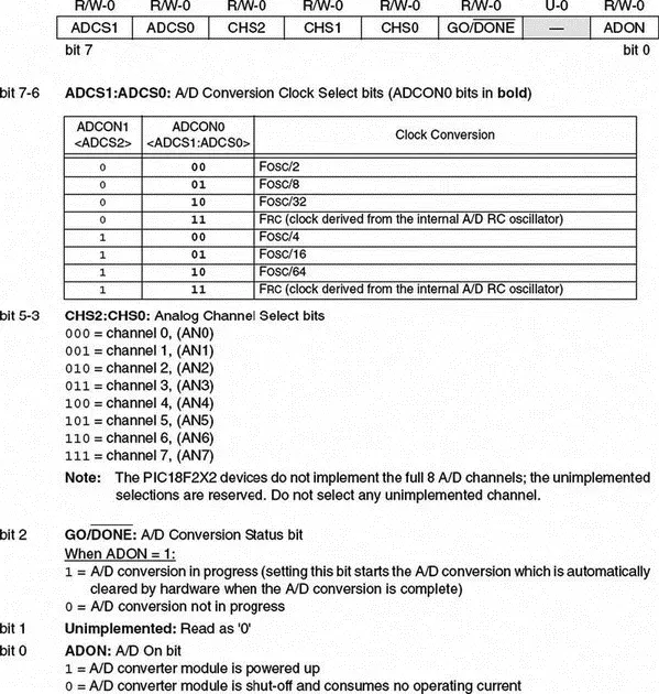
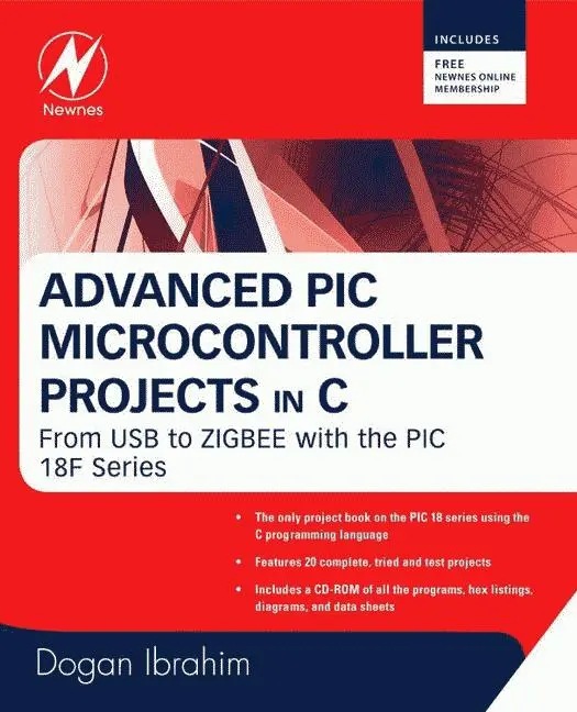
Figure 2.42: ADCON0 register
Register ADCON1 (see Figure 2.43) is used for selecting the conversion format, configuring the A/D channels for analog input, selecting the reference voltage, and selecting the conversion clock together with register ADCON0.
Figure 2.43: ADCON1 register
A/D conversion starts by setting the GO/DONE bit of ADCON0. When the conversion is complete, the 2 bits of the converted data is written into register ADRESH, and the remaining 8 bits are written into register ADRESL. At the same time the GO/DONE bit is cleared to indicate the end of conversion. If required, interrupts can be enabled so that a software interrupt is generated when the conversion is complete.
The steps in carrying out an A/D conversion are as follows:
• Use ADCON1 to configure required channels as analog and configure the reference voltage.
• Set the TRISA or TRISE bits so the required channel is an input port.
• Use ADCON0 to select the required analog input channel.
• Use ADCON0 and ADCON1 to select the conversion clock.
• Use ADCON0 to turn on the A/D module.
• Configure the A/D interrupt (if desired).
• Set the GO/DONE bit to start conversion.
• Wait until the GO/DONE bit is cleared, or until a conversion complete interrupt is generated.
• Read the converted data from ADRESH and ADRESL.
• Repeat these steps as required.
For correct A/D conversion, the A/D conversion clock must be selected to ensure a minimum bit conversion time of 1.6μs. Table 2.11 gives the recommended A/D clock sources for various microcontroller operating frequencies. For example, if the microcontroller is operated from a 10MHz clock, the A/D clock source should be F OSC/16or higher (e.g., F OSC/32).
Table 2.11: A/D conversion clock selection
| A/D clock source | ||
|---|---|---|
| Operation | ADCS2:ADCS0 | Maximum microcontroller frequency |
| 2 T OSC | 000 | 1.25 MHz |
| 4 T OSC | 100 | 2.50 MHz |
| 8 T OSC | 001 | 5.0 MHz |
| 16 T OSC | 101 | 10.0 MHz |
| 32 T OSC | 010 | 20.0 MHz |
| 64 T OSC | 110 | 40.0 MHz |
| RC | 011 | – |
Bit ADFM of register ADCON1 controls the format of a conversion. When ADFM is cleared, the 10-bit result is left justified (see Figure 2.44) and lower 6 bits of ADRESL are cleared to 0. When ADFM is set to 1 the result is right justified and the upper 6 bits of ADRESH are cleared to 0. This is the mode most commonly used, in which ADRESL contains the lower 8 bits, and bits 0 and 1 of ADRESH contain the upper 2 bits of the 10-bit result.
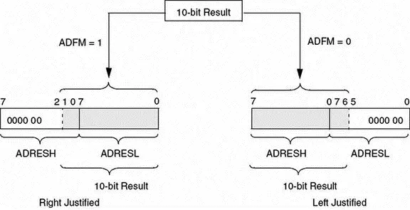
Figure 2.44: Formatting the A/D conversion result
An understanding of the A/D analog input model is necessary to interface the A/D to external devices. Figure 2.45 shows the analog input model of the A/D. The analog input voltage V AINand the source resistance R Sare shown on the left side of the diagram. It is recommended that the source resistance be no greater than 2.5K. The analog signal is applied to the pin labeled ANx. There is a small capacitance (5pF) and a leakage current to the ground of approximately 500nA. R ICis the interconnect resistance, which has a value of less than 1K. The sampling process is shown with switch SS having a resistance R SSwhose value depends on the voltage as shown in the small graph at the bottom of Figure 2.45. The value of R SSis approximately 7K at 5V supply voltage.
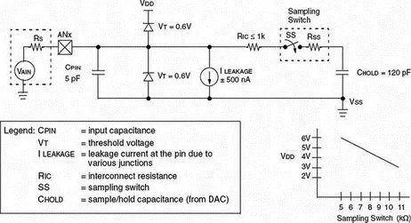
Figure 2.45: Analog input model of the A/D converter
The A/D converter is based on a switched capacitor principle, and capacitor C HOLDshown in Figure 2.45 must be charged fully before the start of a conversion. This is a 120pF capacitor which is disconnected from the input pin once the conversion is started.
The acquisition time can be calculated by using Equation (2.7), provided by Microchip Inc:
T ACQ = Amplifier settling time + Holding capacitor charging time + temperature coefficient (2.7)
The amplifier settling time is specified as a fixed 2μs. The temperature coefficient, which is only applicable if the temperature is above 25°C, is specified as:
Temperature coefficient = (Temperature – 25°C)(0.05μs/°C) (2.8)
Equation (2.8) shows that the effect of the temperature is very small, creating about 0.5μs delay for every 10°C above 25°C. Thus, assuming a working environment between 25°C and 35°C, the maximum delay due to temperature will be 0.5μs, which can be ignored for most practical applications.
The holding capacitor charging time as specified by Microchip Inc is:
Holding capacitor charging time = –(120pF)(1K + R SS + R S)Ln(1/2048) (2.9)
Assuming that R SS= 7K, R S= 2.5K, Equation (2.9) gives the holding capacitor charging time as 9.6μs.
The acquisition time is then calculated as:
T ACQ = 2 + 9.6 + 0.5 = 12.1μs
A full 10-bit conversion takes 12 A/D cycles, and each A/D cycle is specified at a minimum of 1.6μs. Thus, the fastest conversion time is 19.2μs. Adding this to the best possible acquisition time gives a total time to complete a conversion of 19.2+12.1=31.3μs.
When a conversion is complete, it is specified that the converter should wait for two conversion periods before starting a new conversion. This corresponds to 2×1.6=3.2μs. Adding this to the best possible conversion time of 31.3μs gives a complete conversion time of 34.5μs. Assuming the A/D converter is used successively, and ignoring the software overheads, this implies a maximum sampling frequency of about 29KHz.
2.1.12 Interrupts
An interrupt is an event that requires the CPU to stop normal program execution and then execute a program code related to the event causing the interrupt. Interrupts can be generated internally (by some event inside the chip) or externally (by some external event). An example of an internal interrupt is a timer overflowing or the A/D completing a conversion. An example of an external interrupt is an I/O pin changing state.
Interrupts can be useful in many applications such as:
• Time critical applications. Applications which require the immediate attention of the CPU can use interrupts. For example, in an emergency such as a power failure or fire in a plant the CPU may have to shut down the system immediately in an orderly manner. In such applications an external interrupt can force the CPU to stop whatever it is doing and take immediate action.
• Performing routine tasks. Many applications require the CPU to perform routine work at precise times, such as checking the state of a peripheral device exactly every millisecond. A timer interrupt scheduled with the required timing can divert the CPU from normal program execution to accomplish the task at the precise time required.
• Task switching in multi-tasking applications. In multi-tasking applications, each task may have a finite time to execute its code. Interrupt mechanisms can be used to stop a task should it consume more than its allocated time.
Читать дальшеИнтервал:
Закладка:
Похожие книги на «Advanced PIC Microcontroller Projects in C»
Представляем Вашему вниманию похожие книги на «Advanced PIC Microcontroller Projects in C» списком для выбора. Мы отобрали схожую по названию и смыслу литературу в надежде предоставить читателям больше вариантов отыскать новые, интересные, ещё непрочитанные произведения.


Обсуждение, отзывы о книге «Advanced PIC Microcontroller Projects in C» и просто собственные мнения читателей. Оставьте ваши комментарии, напишите, что Вы думаете о произведении, его смысле или главных героях. Укажите что конкретно понравилось, а что нет, и почему Вы так считаете.