Ibrahim Dogan - Advanced PIC Microcontroller Projects in C
Здесь есть возможность читать онлайн «Ibrahim Dogan - Advanced PIC Microcontroller Projects in C» весь текст электронной книги совершенно бесплатно (целиком полную версию без сокращений). В некоторых случаях можно слушать аудио, скачать через торрент в формате fb2 и присутствует краткое содержание. Город: Burlington, Год выпуска: 2008, ISBN: 2008, Издательство: Elsevier Ltd, Жанр: Программирование, Компьютерное железо, на английском языке. Описание произведения, (предисловие) а так же отзывы посетителей доступны на портале библиотеки ЛибКат.
- Название:Advanced PIC Microcontroller Projects in C
- Автор:
- Издательство:Elsevier Ltd
- Жанр:
- Год:2008
- Город:Burlington
- ISBN:978-0-7506-8611-2
- Рейтинг книги:5 / 5. Голосов: 1
-
Избранное:Добавить в избранное
- Отзывы:
-
Ваша оценка:
Advanced PIC Microcontroller Projects in C: краткое содержание, описание и аннотация
Предлагаем к чтению аннотацию, описание, краткое содержание или предисловие (зависит от того, что написал сам автор книги «Advanced PIC Microcontroller Projects in C»). Если вы не нашли необходимую информацию о книге — напишите в комментариях, мы постараемся отыскать её.
• Features 20 complete, tried and test projects
• Includes a CD-ROM of all the programs, hex listings, diagrams, and data sheets
Advanced PIC Microcontroller Projects in C — читать онлайн бесплатно полную книгу (весь текст) целиком
Ниже представлен текст книги, разбитый по страницам. Система сохранения места последней прочитанной страницы, позволяет с удобством читать онлайн бесплатно книгу «Advanced PIC Microcontroller Projects in C», без необходимости каждый раз заново искать на чём Вы остановились. Поставьте закладку, и сможете в любой момент перейти на страницу, на которой закончили чтение.
Интервал:
Закладка:
TMR2PS is the Timer 2 prescaler value
T OSCis the clock oscillator period (seconds)
The PWM frequency is defined as 1/(PWM period).
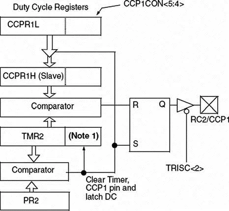
Figure 2.38: PWM module block diagram
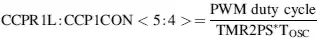
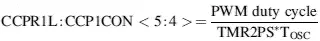
The resolution of the PWM duty cycle is 10 bits. The PWM duty cycle is selected by writing the eight most significant bits into the CCPR1L register and the two least significant bits into bits 4 and 5 of CCP1CON register. The duty cycle (in seconds) is given by:
PWM duty cycle = (CCPR1L:CCP1CON<5:4>) * TMR2PS * T OSC (2.5)
or
 (2.6)
(2.6)
The steps to configure the PWM are as follows:
• Specify the required period and duty cycle.
• Choose a value for the Timer 2 prescaler (TMR2PS).
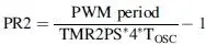
• Calculate the value to be written into the PR2 register using Equation (2.2).
• Calculate the value to be loaded into the CCPR1L and CCP1CON registers using Equation (2.6).
• Clear bit 2 of TRISC to make CCP1 pin an output pin.
• Configure the CCP1 module for PWM operation using register CCP1CON.
The following example shows how the PWM can be set up.
PWM pulses must be generated from pin CCP1 of a PIC18F452 microcontroller. The required pulse period is 44ms and the required duty cycle is 50%. Assuming that the microcontroller operates with a 4MHz crystal, calculate the values to be loaded into the various registers.
Using a 4MHz crystal; T OSC = 1/4 = 0.25 × 10 –6
The required PWM duty cycle is 44/2 = 22μs.
From Equation (2.4), assuming a timer prescaler factor of 4, we have:
or
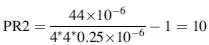 i.e., 0AH
and from Equation (2.6)
or
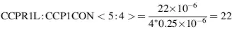
But the equivalent of number 22 in 10-bit binary is:
“00 00010110”
Therefore, the value to be loaded into bits 4 and 5 of CCP1CON is “00.” Bits 2 and 3 of CCP1CON must be set to high for PWM operation. Therefore, CCP1CON must be set to bit pattern (“X” is “don’t care”):
XX001100
Taking the don’t-care entries as 0, we can set CCP1CON to hexadecimal 0CH.
The value to be loaded into CCPR1L is “00010110” (i.e., hexadecimal number 16H). The required steps are summarized as follows:
• Load Timer 2 with prescaler of 4 (i.e., load T2CON) with 00000101 (i.e., 05H).
• Load 0AH into PR2.
• Load 16H into CCPR1L.
• Load 0 into TRISC (make CCP1 pin output).
• Load 0CH into CCP1CON.
One period of the generated PWM waveform is shown in Figure 2.39.
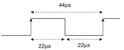
Figure 2.39: Generated PWM waveform
2.1.11 Analog-to-Digital Converter (A/D) Module
An analog-to-digital converter (A/D) is another important peripheral component of a microcontroller. The A/D converts an analog input voltage into a digital number so it can be processed by a microcontroller or any other digital system. There are many analog-to-digital converter chips available on the market, and an embedded systems designer should understand the characteristics of such chips so they can be used efficiently.
As far as the input and output voltage are concerned A/D converters can be classified as either unipolar and bipolar. Unipolar A/D converters accept unipolar input voltages in the range 0 to +0V, and bipolar A/D converters accept bipolar input voltages in the range ±V. Bipolar converters are frequently used in signal processing applications, where the signals by nature are bipolar. Unipolar converters are usually cheaper, and they are used in many control and instrumentation applications.
Figure 2.40 shows the typical steps involved in reading and converting an analog signal into digital form, a process also known as signal conditioning. Signals received from sensors usually need to be processed before being fed to an A/D converter. This processing usually begins with scaling the signal to the correct value. Unwanted signal components are then removed by filtering the signal using classical filters (e.g., a low-pass filter). Finally, before feeding the signal to an A/D converter, the signal is passed through a sample-and-hold device. This is particularly important with fast real-time signals whose value may be changing between the sampling instants. A sample-and-hold device ensures that the signal stays at a constant value during the actual conversion process. Many applications required more than one A/D, which normally involves using an analog multiplexer at the input of the A/D. The multiplexer selects only one signal at any time and presents this signal to the A/D converter. An A/D converter usually has a single analog input and a digital parallel output. The conversion process is as follows:
• Apply the processed signal to the A/D input
• Start the conversion
• Wait until conversion is complete
• Read the converted digital data
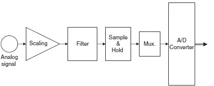
Figure 2.40: Signal conditioning and A/D conversion process
The A/D conversion starts by triggering the converter. Depending on the speed of the converter, the conversion process itself can take several microseconds. At the end of the conversion, the converter either raises a flag or generates an interrupt to indicate that the conversion is complete. The converted parallel output data can then be read by the digital device connected to the A/D converter.
Most members of the PIC18F family contain a 10-bit A/D converter. If the chosen voltage reference is +5V, the voltage step value is:
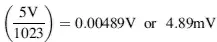
Therefore, for example, if the input voltage is 1.0V, the converter will generate a digital output of 1.0/0.00489 = 205 decimal. Similarly, if the input voltage is 3.0V, the converter will generate 3.0/0.00489 = 613.
The A/D converter used by the PIC18F452 microcontroller has eight channels, named AN0–AN7, which are shared by the PORTA and PORTE pins. Figure 2.41 shows the block diagram of the A/D converter.
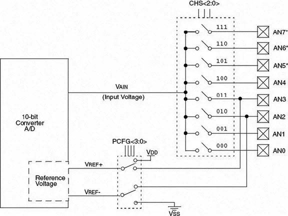
Figure 2.41: Block diagram of the PIC18F452 A/D converter
The A/D converter has four registers. Registers ADRESH and ADRESL store the higher and lower results of the conversion respectively. Register ADCON0, shown in Figure 2.42, controls the operation of the A/D module, such as selecting the conversion clock together with register ADCON1, selecting an input channel, starting a conversion, and powering up and shutting down the A/D converter.
Читать дальшеИнтервал:
Закладка:
Похожие книги на «Advanced PIC Microcontroller Projects in C»
Представляем Вашему вниманию похожие книги на «Advanced PIC Microcontroller Projects in C» списком для выбора. Мы отобрали схожую по названию и смыслу литературу в надежде предоставить читателям больше вариантов отыскать новые, интересные, ещё непрочитанные произведения.


Обсуждение, отзывы о книге «Advanced PIC Microcontroller Projects in C» и просто собственные мнения читателей. Оставьте ваши комментарии, напишите, что Вы думаете о произведении, его смысле или главных героях. Укажите что конкретно понравилось, а что нет, и почему Вы так считаете.