Ibrahim Dogan - Advanced PIC Microcontroller Projects in C
Здесь есть возможность читать онлайн «Ibrahim Dogan - Advanced PIC Microcontroller Projects in C» весь текст электронной книги совершенно бесплатно (целиком полную версию без сокращений). В некоторых случаях можно слушать аудио, скачать через торрент в формате fb2 и присутствует краткое содержание. Город: Burlington, Год выпуска: 2008, ISBN: 2008, Издательство: Elsevier Ltd, Жанр: Программирование, Компьютерное железо, на английском языке. Описание произведения, (предисловие) а так же отзывы посетителей доступны на портале библиотеки ЛибКат.
- Название:Advanced PIC Microcontroller Projects in C
- Автор:
- Издательство:Elsevier Ltd
- Жанр:
- Год:2008
- Город:Burlington
- ISBN:978-0-7506-8611-2
- Рейтинг книги:5 / 5. Голосов: 1
-
Избранное:Добавить в избранное
- Отзывы:
-
Ваша оценка:
Advanced PIC Microcontroller Projects in C: краткое содержание, описание и аннотация
Предлагаем к чтению аннотацию, описание, краткое содержание или предисловие (зависит от того, что написал сам автор книги «Advanced PIC Microcontroller Projects in C»). Если вы не нашли необходимую информацию о книге — напишите в комментариях, мы постараемся отыскать её.
• Features 20 complete, tried and test projects
• Includes a CD-ROM of all the programs, hex listings, diagrams, and data sheets
Advanced PIC Microcontroller Projects in C — читать онлайн бесплатно полную книгу (весь текст) целиком
Ниже представлен текст книги, разбитый по страницам. Система сохранения места последней прочитанной страницы, позволяет с удобством читать онлайн бесплатно книгу «Advanced PIC Microcontroller Projects in C», без необходимости каждый раз заново искать на чём Вы остановились. Поставьте закладку, и сможете в любой момент перейти на страницу, на которой закончили чтение.
Интервал:
Закладка:
Table 2.12: PIC18F452 interrupt bits and registers
| Interrupt source | Flag bit | Enable bit | Priority bit |
|---|---|---|---|
| INT0 external | INT0IF | INT0IE | – |
| INT1 external | INT1IF | INT1IE | INT1IP |
| INT2 external | INT2IF | INT2IE | INT2IP |
| RB port change | RBIF | RBIE | RBIP |
| TMR0 overflow | TMR0IF | TMR0IE | TMR0IP |
| TMR1 overflow | TMR1IF | TMR1IE | TMR1IP |
| TMR2 match PR2 | TMR2IF | TMR2IE | TMR2IP |
| TMR3 overflow | TMR3IF | TMR3IE | TMR3IP |
| A/D complete | ADIF | ADIE | ADIP |
| CCP1 | CCP1IF | CCP1IE | CCP1IP |
| CCP2 | CCP2IF | CCP2IE | CCP2IP |
| USART RCV | RCIF | RCIE | RCIP |
| USART TX | TXIF | TXIE | TXIP |
| Parallel slave port | PSPIF | PSPIE | PSPIP |
| Sync serial port | SSPIF | SSPIE | SSPIP |
| Low-voltage detect | LVDIF | LVDIE | LVDIP |
| Bus collision | BCLIF | BCLIE | BCLIP |
| EEPROM/FLASH write | EEIF | EEIE | EEIP |
Figures 2.48 to 2.55 show the bit definitions of interrupt registers INTCON2, INTCON3, PIR1, PIR2, PIE1, PIE2, IPR1, and IPR2.
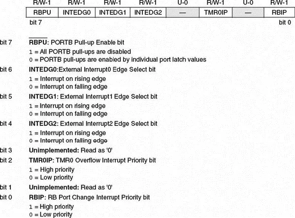
Figure 2.48: INTCON2 bit definitions
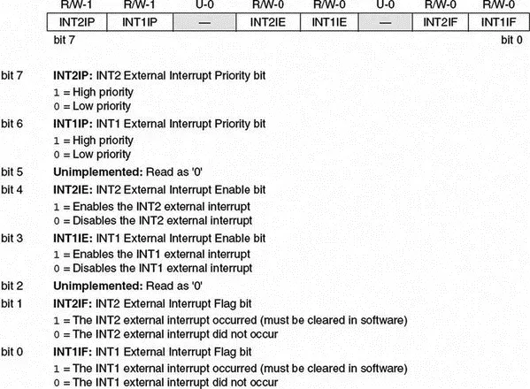
Figure 2.49: INTCON3 bit definitions
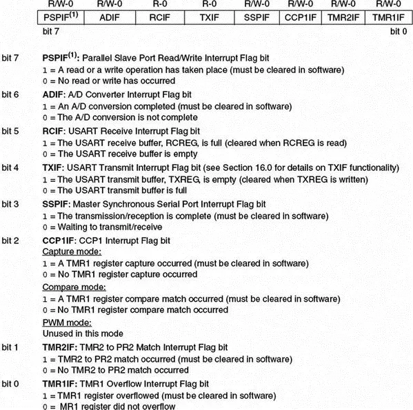
Figure 2.50: PIR1 bit definitions
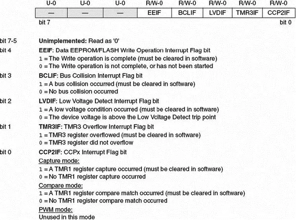
Figure 2.51: PIR2 bit definitions
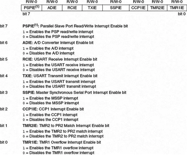
Figure 2.52: PIE1 bit definitions
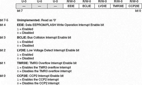
Figure 2.53: PIE2 bit definitions
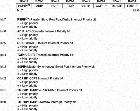
Figure 2.54: IPR1 bit definitions
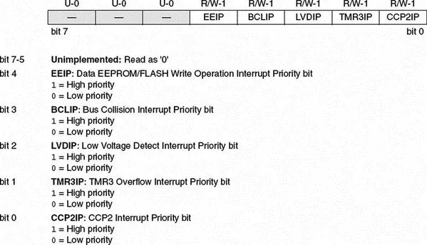
Figure 2.55: IPR2 bit definitions
Examples are given in this section to illustrate how the CPU can be programmed for an interrupt.
Set up INT1 as a falling-edge triggered interrupt input having low priority.
The following bits should be set up before the INT1 falling-edge triggered interrupts can be accepted by the CPU in low-priority mode:
• Enable the priority structure. Set IPEN = 1
• Make INT1 an input pin. Set TRISB = 1
• Set INT1 interrupts for falling edge. SET INTEDG1 = 0
• Enable INT1 interrupts. Set INT1IE = 1
• Enable low priority. Set INT1IP = 0
• Clear INT1 flag. Set INT1IF = 0
• Enable low-priority interrupts. Set GIEL = 1
• Enable all interrupts. Set GIEH = 1
When an interrupt occurs, the CPU jumps to address 00008H in the program memory to execute the user program at the interrupt service routine.
Set up INT1 as a rising-edge triggered interrupt input having high priority.
The following bits should be set up before the INT1 rising-edge triggered interrupts can be accepted by the CPU in high-priority mode:
• Enable the priority structure. Set IPEN = 1
• Make INT1 an input pin. Set TRISB = 1
• Set INT1 interrupts for rising edge. SET INTEDG1 = 1
• Enable INT1 interrupts. Set INT1IE = 1
• Enable high priority. Set INT1IP = 1
• Clear INT1 flag. Set INT1IF = 0
• Enable all interrupts. Set GIEH = 1
When an interrupt occurs, the CPU jumps to address 000018H of the program memory to execute the user program at the interrupt service routine.
2.2 Summary
This chapter has described the architecture of the PIC18F family of microcontrollers. The PIC18F452 was used as a typical sample microcontroller in this family. Other members of the same family, such as the PIC18F242, have smaller pin counts and less functionality. And some, such as the PIC18F6680, have larger pin counts and more functionality.
Important parts and peripheral circuits of the PIC18F series have been described, including data memory, program memory, clock circuits, reset circuits, watchdog timer, general purpose timers, capture and compare module, PWM module, A/D converter, and the interrupt structure.
2.3 Exercises
1. Describe the data memory structure of the PIC18F452 microcontroller. What is a bank? How many banks are there?
2. Explain the differences between a general purpose register (GPR) and a special function register (SFR).
3. Explain the various ways the PIC18F microcontroller can be reset. Draw a circuit diagram to show how an external push-button switch can be used to reset the microcontroller.
4. Describe the various clock sources that can be used to provide a clock to a PIC18F452 microcontroller. Draw a circuit diagram to show how a 10MHz crystal can be connected to the microcontroller.
5. Draw a circuit diagram to show how a resonator can be connected to a PIC18F microcontroller.
6. In a non-time-critical application a clock must be provided for a PIC18F452 microcontroller using an external resistor and a capacitor. Draw a circuit diagram to show how this can be done and find the component values for a required clock frequency of 5MHz.
7. Explain how an external clock can provide clock pulses to a PIC18F microcontroller.
8. What are the registers of PORTA? Explain the operation of the port by drawing the port block diagram.
9. The watchdog timer must be set to provide an automatic reset every 0.5 seconds. Describe how to do this, including the appropriate register bits.
10. PWM pulses must be generated from pin CCP1 of a PIC18F452 microcontroller. The required pulse period is 100ms, and the required duty cycle is 50%. Assuming the microcontroller is operating with a 4MHz crystal, calculate the values to be loaded into the various registers.
11. Again, with regard to PWM pulses generated from pin CCP1 of a PIC18F452 microcontroller: If the required pulse frequency is 40KHz, and the required duty cycle is 50%, and assuming the microcontroller is operating with a 4MHz crystal, calculate the values to be loaded into the various registers.
12. An LM35DZ-type analog temperature sensor is connected to analog port AN0 of a PIC18F452 microcontroller. The sensor provides an analog output voltage proportional to the temperature (i.e., V0 = 10 mV/°C). Show the steps required to read the temperature.
13. Explain the difference between a priority interrupt and a nonpriority interrupt.
14. Show the steps required to set up INT2 as a falling-edge triggered interrupt input having low priority. What is the interrupt vector address?
Читать дальшеИнтервал:
Закладка:
Похожие книги на «Advanced PIC Microcontroller Projects in C»
Представляем Вашему вниманию похожие книги на «Advanced PIC Microcontroller Projects in C» списком для выбора. Мы отобрали схожую по названию и смыслу литературу в надежде предоставить читателям больше вариантов отыскать новые, интересные, ещё непрочитанные произведения.


Обсуждение, отзывы о книге «Advanced PIC Microcontroller Projects in C» и просто собственные мнения читателей. Оставьте ваши комментарии, напишите, что Вы думаете о произведении, его смысле или главных героях. Укажите что конкретно понравилось, а что нет, и почему Вы так считаете.