Ibrahim Dogan - Advanced PIC Microcontroller Projects in C
Здесь есть возможность читать онлайн «Ibrahim Dogan - Advanced PIC Microcontroller Projects in C» весь текст электронной книги совершенно бесплатно (целиком полную версию без сокращений). В некоторых случаях можно слушать аудио, скачать через торрент в формате fb2 и присутствует краткое содержание. Город: Burlington, Год выпуска: 2008, ISBN: 2008, Издательство: Elsevier Ltd, Жанр: Программирование, Компьютерное железо, на английском языке. Описание произведения, (предисловие) а так же отзывы посетителей доступны на портале библиотеки ЛибКат.
- Название:Advanced PIC Microcontroller Projects in C
- Автор:
- Издательство:Elsevier Ltd
- Жанр:
- Год:2008
- Город:Burlington
- ISBN:978-0-7506-8611-2
- Рейтинг книги:5 / 5. Голосов: 1
-
Избранное:Добавить в избранное
- Отзывы:
-
Ваша оценка:
Advanced PIC Microcontroller Projects in C: краткое содержание, описание и аннотация
Предлагаем к чтению аннотацию, описание, краткое содержание или предисловие (зависит от того, что написал сам автор книги «Advanced PIC Microcontroller Projects in C»). Если вы не нашли необходимую информацию о книге — напишите в комментариях, мы постараемся отыскать её.
• Features 20 complete, tried and test projects
• Includes a CD-ROM of all the programs, hex listings, diagrams, and data sheets
Advanced PIC Microcontroller Projects in C — читать онлайн бесплатно полную книгу (весь текст) целиком
Ниже представлен текст книги, разбитый по страницам. Система сохранения места последней прочитанной страницы, позволяет с удобством читать онлайн бесплатно книгу «Advanced PIC Microcontroller Projects in C», без необходимости каждый раз заново искать на чём Вы остановились. Поставьте закладку, и сможете в любой момент перейти на страницу, на которой закончили чтение.
Интервал:
Закладка:
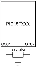
Figure 2.15: Using a resonator as the clock input
The LP (low-power) oscillator mode is advised in applications to up to 200KHz clock. The XT mode is advised to up to 4MHz, and the HS (high-speed) mode is advised in applications where the clock frequency is between 4MHz to 25MHz.
An external clock source may also be connected to the OSC1 pin in the LP, XT, or HS modes as shown in Figure 2.16.
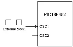
Figure 2.16: Connecting an external clock in LP, XT, or HS modes
An external clock source can be connected to the OSC1 input of the microcontroller in EC and ECIO modes. No oscillator start-up time is required after a power-on reset. Figure 2.17 shows the operation with the external clock in EC mode. Timing pulses at the frequency FOSC/4 are available on the OSC2 pin. These pulses can be used for test purposes or to provide pulses to external devices.
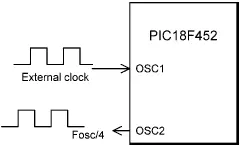
Figure 2.17: External clock in EC mode
The ECIO mode is similar to the EC mode, except that the OSC2 pin can be used as a general purpose digital I/O pin. As shown in Figure 2.18, this pin becomes bit 6 of PORTA (i.e., pin RA6).
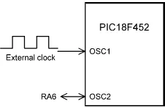
Figure 2.18: External clock in ECIO mode
In the many applications where accurate timing is not required we can use an external resistor and a capacitor to provide clock pulses. The clock frequency is a function of the resistor, the capacitor, the power supply voltage, and the temperature. The clock frequency is not accurate and can vary from unit to unit due to manufacturing and component tolerances. Table 2.5 gives the approximate clock frequency with various resistor and capacitor combinations. A close approximation of the clock frequency is 1/(4.2RC), where R should be between 3K and 100K and C should be greater than 20pF.
Table 2.5: Clock frequency with RC
| C (pF) | R (K) | Frequency (MHz) |
|---|---|---|
| 22 | 3.3 | 3.3 |
| 4.7 | 2.3 | |
| 10 | 1.08 | |
| 30 | 3.3 | 2.4 |
| 4.7 | 1.7 | |
| 10 | 0.793 |
In RC mode, the oscillator frequency divided by 4 (FOSC/4) is available on pin OSC2 of the microcontroller. Figure 2.19 shows the operation at a clock frequency of approximately 2MHz, where R=3.9K and C=30pF. In this application the clock frequency at the output of OSC2 is 2MHz/4=500KHz.
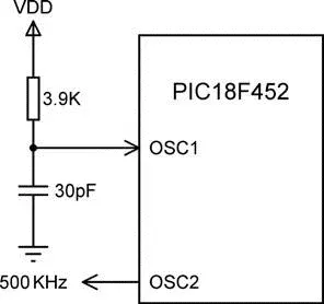
Figure 2.19: 2MHz clock in RC mode
RCIO mode is similar to RC mode, except that the OSC2 pin can be used as a general purpose digital I/O pin. As shown in Figure 2.20, this pin becomes bit 6 of PORTA (i.e., pin RA6).
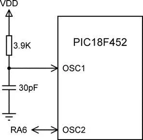
Figure 2.20: 2MHz clock in RCIO mode
One of the problems with using high-frequency crystals or resonators is electromagnetic interference. A Phase Locked Loop (PLL) circuit is provided that can be enabled to multiply the clock frequency by 4. Thus, for a crystal clock frequency of 10MHz, the internal operation frequency will be multiplied to 40MHz. The PLL mode is enabled when the oscillator configuration bits are programmed for HS mode.
Some devices in the PIC18F family have internal clock modes (although the PIC18F452 does not). In this mode, OSC1 and OSC2 pins are available for general purpose I/O (RA6 and RA7) or as FOSC/4 and RA7. An internal clock can be from 31KHz to 8MHz and is selected by registers OSCCON and OSCTUNE. Figure 2.21 shows the bits of internal clock control registers.
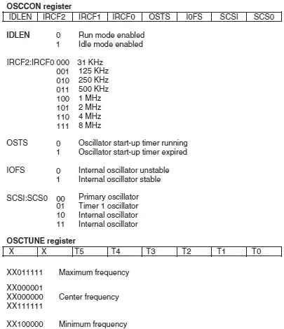
Figure 2.21: Internal clock control registers
It is possible to switch the clock from the main oscillator to a low-frequency clock source. For example, the clock can be allowed to run fast in periods of intense activity and slower when there is less activity. In the PIC18F452 microcontroller this is controlled by bit SCS of the OSCCON register. In microcontrollers of the PIC18F family that do support an internal clock, clock switching is controlled by bits SCS0 and SCS1 of OSCCON. It is important to ensure that during clock switching unwanted glitches do not occur in the clock signal. PIC18F microcontrollers contain circuitry to ensure error-free switching from one frequency to another.
2.1.7 Watchdog Timer
In PIC18F-series microcontrollers family members the watchdog timer (WDT) is a free-running on-chip RC-based oscillator and does not require any external components. When the WDT times out, a device RESET is generated. If the device is in SLEEP mode, the WDT time-out will wake it up and continue with normal operation.
The watchdog is enabled/disabled by bit SWDTEN of register WDTCON. Setting SWDTEN = 1 enables the WDT, and clearing this bit turns off the WDT. On the PIC18F452 microcontroller an 8-bit postscaler is used to multiply the basic time-out period from 1 to 128 in powers of 2. This postscaler is controlled from configuration register CONFIG2H. The typical basic WDT time-out period is 18ms for a postscaler value of 1.
2.1.8 Parallel I/O Ports
The parallel ports in PIC18F microcontrollers are very similar to those of the PIC16 series. The number of I/O ports and port pins varies depending on which PIC18F microcontroller is used, but all of them have at least PORTA and PORTB. The pins of a port are labeled as RPn, where P is the port letter and n is the port bit number. For example, PORTA pins are labeled RA0 to RA7, PORTB pins are labeled RB0 to RB7, and so on.
When working with a port we may want to:
• Set port direction
• Set an output value
• Read an input value
• Set an output value and then read back the output value
The first three operations are the same in the PIC16 and the PIC18F series. In some applications we may want to send a value to the port and then read back the value just sent. The PIC16 series has a weakness in the port design such that the value read from a port may be different from the value just written to it. This is because the reading is the actual port bit pin value, and this value can be changed by external devices connected to the port pin. In the PIC18F series, a latch register (e.g., LATA for PORTA) is introduced to the I/O ports to hold the actual value sent to a port pin. Reading from the port reads the latched value, which is not affected by any external device.
In this section we shall be looking at the general structure of I/O ports.
In the PIC18F452 microcontroller PORTA is 7 bits wide and port pins are shared with other functions. Table 2.6 shows the PORTA pin functions.
Table 2.6: PIC18F452 PORTA pin functions
Читать дальшеИнтервал:
Закладка:
Похожие книги на «Advanced PIC Microcontroller Projects in C»
Представляем Вашему вниманию похожие книги на «Advanced PIC Microcontroller Projects in C» списком для выбора. Мы отобрали схожую по названию и смыслу литературу в надежде предоставить читателям больше вариантов отыскать новые, интересные, ещё непрочитанные произведения.


Обсуждение, отзывы о книге «Advanced PIC Microcontroller Projects in C» и просто собственные мнения читателей. Оставьте ваши комментарии, напишите, что Вы думаете о произведении, его смысле или главных героях. Укажите что конкретно понравилось, а что нет, и почему Вы так считаете.