| Ae |
|
effective antenna aperture |
| c |
speed of light |
| D |
directivity |
| D = max[ D ( ϑ , ϕ )] |
directivity function |
| η |
effciency |
 |
unit vector along the r axis |
 |
electric field in space frequency |
| f |
frequency |
| G |
gain |
| G = max[ G ( ϑ , ϕ )] |
gain function |
| Γ |
reflection coeffcient |
| I p |
input current antenna |
| k |
coverage factor |
| L |
length of the radiating aperture |
| λ 0 |
wavelength in free space |
| Mv |
measurement value |
| Pin |
input power |
| Pt |
total radiated power |
| P ( ϑ , ϕ ) |
normalized radiation power |
| R |
radial distance from the antenna |
| Ra |
resistive |
| RL |
radiated losses |
| Rr |
radiated resistance |
| Rv |
reference value |
| μ sys |
system uncertainty |
 |
Poynting vector |
| V p |
input voltage antenna |
| X a |
reactance |
| Z 0 |
characteristic impedance |
| Z a |
input impedance |
| Z g |
generator impedance = R g |
Yueping Zhang
School of Electrical and Electronic Engineering, Nanyang Technological University, Singapore
As the technology of choice for integration of digital circuitry, a complementary metal oxide semiconductor (CMOS) was proposed for the integration of analog circuitry for radio frequency (RF) applications in the mid‐1980s, aiming for the ultimate goal of full integration of an entire wireless system on a chip [1]. In the mid‐1990s, the first fully integrated CMOS transceiver for data communications in the 900‐MHz industrial, scientific and medical (ISM) band was successfully demonstrated [2]. Since then, CMOS has been the enabler for wireless systems on chip (SoCs) operating from a few to tens of gigahertz. Figure 1.1shows the die micrograph of the first wireless SoC, a 2.4‐GHz CMOS mixed RF analog–digital Bluetooth radio announced at the International Solid‐State Circuits Conference (ISSCC) 2001 [3]. The die size is 40.1 mm 2. It integrates on the same substrate a low intermediate frequency (IF) receiver, a Cartesian transmitter, a baseband processer, an advanced reduced‐instruction set‐computer machine (ARM) processor, flash memory, and random‐access memory (RAM).
Full SoC integration is clearly not suitable in all cases. In fact, the radio chip is separate in many cases. Traditionally, silicon germanium (SiGe) seems to have been preferred to CMOS for analog RF. Figure 1.2shows the die micrographs of the first SiGe 60‐GHz transmitter and receiver disclosed at ISSCC 2006 [4]. The die sizes are 4.0 × 1.6 mm 2and 3.4 × 1.7 mm 2, respectively. The level of integration achieved in these chips was high then for 60‐GHz radios. The transmitter chip integrates a power amplifier, image‐reject driver, IF‐to‐RF up‐mixer, IF amplifiers, quadrature baseband‐to‐IF mixers, phase‐locked loop (PLL), and frequency tripler. The receiver chip includes an image‐reject low‐noise amplifier, RF‐to‐IF mixer, IF amplifiers, quadrature IF‐to‐baseband mixers, PLL, and frequency tripler. The input/output (I/O) pads are peripheral, with 60 on the transmitter and 53 on the receiver chips.
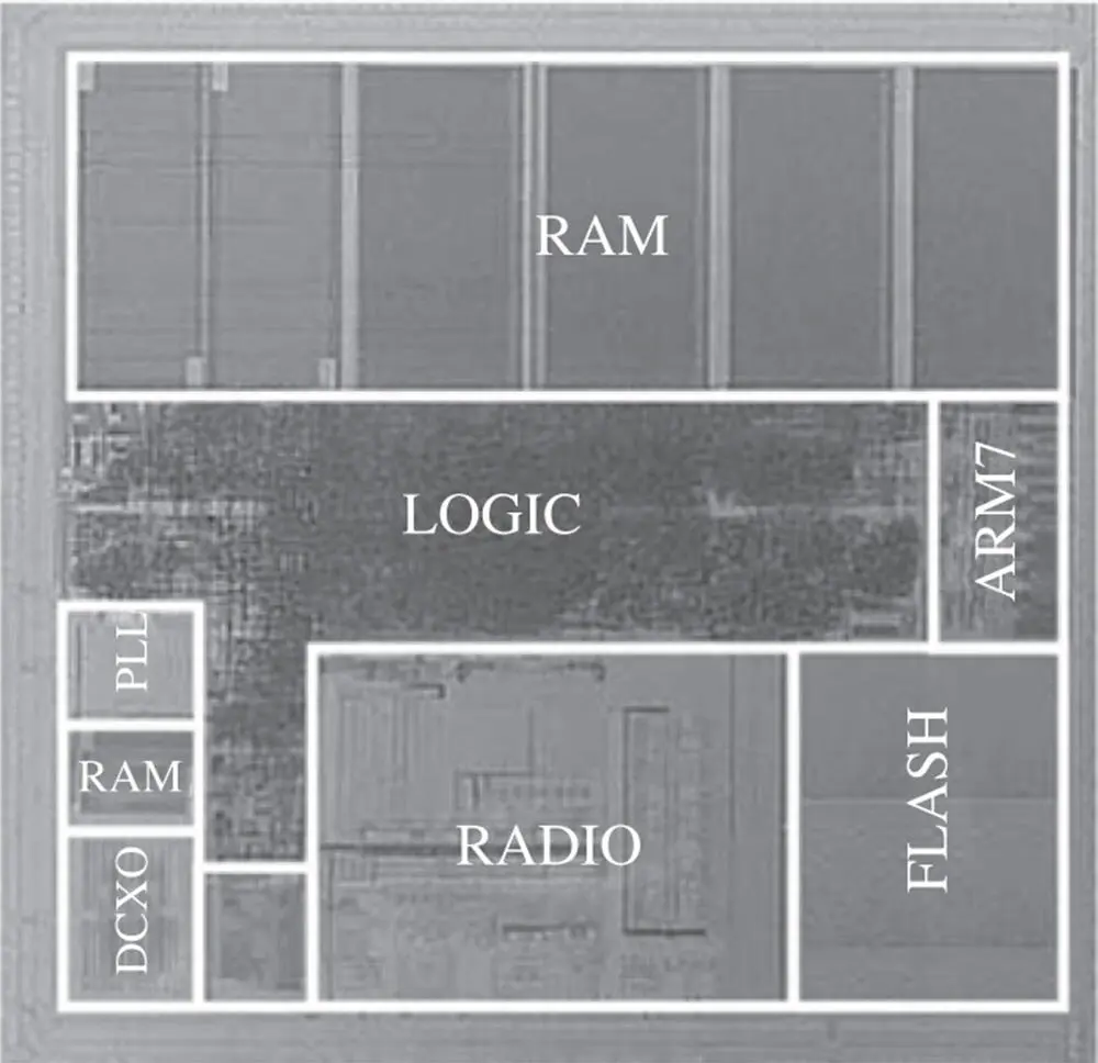 Figure 1.1 Micrograph of the first 2.4‐GHz CMOS wireless SoC, a Bluetooth radio (from [3], © 2001 IEEE, reprinted with permission).
 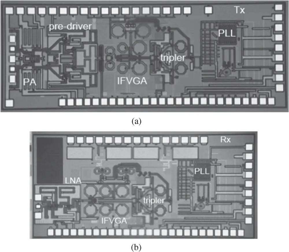 Figure 1.2 Photographs of the first 60‐GHz SiGe radio chipset: (a) transmitter and (b) receiver (from [4], © 2006 IEEE, reprinted with permission).
The emergence of wireless SoCs or single‐chip radios called for compatible antenna solutions, which provided an excellent opportunity for researchers of prepared minds to seriously explore the feasibility of integrating an antenna in a chip package using packaging materials and processes in the late 1990s, leading to the development of antenna‐in‐package (AiP) technology [5]. This chapter recounts how AiP technology has been developed to its current state. Section 1.2describes the idea of AiP with respect to the ideas of antenna on chip (AoC), antenna in module (AiM), antenna on board (AoB), and active integrated antenna (AIA). Section 1.3reviews the early attempts to explore the idea of AiP. Section 1.4reflects on the milestones in the development of the idea of AiP into a mainstream antenna and packaging technology. Finally, Section 1.5gives concluding remarks.
The idea of AiP was triggered by the demand for innovative antenna solutions to wireless SoCs [6]. It features using packaging technology to implement an antenna (or antennas) with a radio or radar die (or dies) in a chip package. It emphasizes only the addition of the unique function of radiation to the package. In this sense, it is different from the concept of system‐in‐package (SiP).
The idea of AoC sounds attractive [7]. It attempts to integrate an antenna (or antennas) with other circuits on a die directly using semiconductor technology. It is obviously a subset of the concept of SoC. Then why do we specifically differentiate it from SoC? The reason is to highlight the unique property of radiation, which is not necessarily being improved like digital circuits as the technology scales down. It is clear that AoC is more suitable for terahertz applications for cost and performance reasons.
The idea of AiM was proposed for multichip 60‐GHz radios [8]. It uses micro‐assembly technology to mount a few monolithic microwave integrated circuits (MMICs) and a small flat antenna in a hermetically sealed package. A window for the propagation of electromagnetic waves is formed above the antenna at the lid of the package. The window is also hermetically sealed.
The idea of AoB is similar to the idea of AiP. However, it relies on printed circuit board (PCB) technology to make an antenna (or antennas) on one surface of a board and to solder a packaged chip (or chips) on the other surface of the board. A few techniques, such as probe feeding or aperture coupling, are available to interconnect the packaged chip with the antenna. Of course, the antenna, the packaged chip, and the necessary feed networks can be contained on the same surface of the board. Recently, the idea of AoB has received considerable attention for millimeter‐wave (mmWave) fifth‐generation (5G) base stations [9].
Читать дальше



 Figure 1.1 Micrograph of the first 2.4‐GHz CMOS wireless SoC, a Bluetooth radio (from [3], © 2001 IEEE, reprinted with permission).
  Figure 1.2 Photographs of the first 60‐GHz SiGe radio chipset: (a) transmitter and (b) receiver (from [4], © 2006 IEEE, reprinted with permission).