King-Ning Tu - Electronic Packaging Science and Technology
Здесь есть возможность читать онлайн «King-Ning Tu - Electronic Packaging Science and Technology» — ознакомительный отрывок электронной книги совершенно бесплатно, а после прочтения отрывка купить полную версию. В некоторых случаях можно слушать аудио, скачать через торрент в формате fb2 и присутствует краткое содержание. Жанр: unrecognised, на английском языке. Описание произведения, (предисловие) а так же отзывы посетителей доступны на портале библиотеки ЛибКат.
- Название:Electronic Packaging Science and Technology
- Автор:
- Жанр:
- Год:неизвестен
- ISBN:нет данных
- Рейтинг книги:4 / 5. Голосов: 1
-
Избранное:Добавить в избранное
- Отзывы:
-
Ваша оценка:
Electronic Packaging Science and Technology: краткое содержание, описание и аннотация
Предлагаем к чтению аннотацию, описание, краткое содержание или предисловие (зависит от того, что написал сам автор книги «Electronic Packaging Science and Technology»). Если вы не нашли необходимую информацию о книге — напишите в комментариях, мы постараемся отыскать её.
The electronics industry is shifting towards system packaging technology due to the need for higher chip circuit density without increasing production costs. Electronic packaging, or circuit integration, is seen as a necessary strategy to achieve a performance growth of electronic circuitry in next-generation electronics. With the implementation of novel materials with specific and tunable electrical and magnetic properties, electronic packaging is highly attractive as a solution to achieve denser levels of circuit integration.
The first part of the book gives an overview of electronic packaging and provides the reader with the fundamentals of the most important packaging techniques such as wire bonding, tap automatic bonding, flip chip solder joint bonding, microbump bonding, and low temperature direct Cu-to-Cu bonding. Part two consists of concepts of electronic circuit design and its role in low power devices, biomedical devices, and circuit integration. The last part of the book contains topics based on the science of electronic packaging and the reliability of packaging technology.
Electronic Packaging Science and Technology — читать онлайн ознакомительный отрывок
Ниже представлен текст книги, разбитый по страницам. Система сохранения места последней прочитанной страницы, позволяет с удобством читать онлайн бесплатно книгу «Electronic Packaging Science and Technology», без необходимости каждый раз заново искать на чём Вы остановились. Поставьте закладку, и сможете в любой момент перейти на страницу, на которой закончили чтение.
Интервал:
Закладка:
About the increase of I/O, from BGA to C‐4 joints, there is a RDL of Cu wires in the upper part of the polymer board. From C‐4 joints to μ‐bumps, there is an RDL of Cu wires at the lower part of the interposer chip. This second RDL is invisible in the figure, but it is new in 3D IC because it does not exist in 2D IC devices, where typically there are only two levels of solder joints. The failure of the new RDL is of concern.
Figure 1.5a and b show synchrotron radiation tomographic images of a 3D IC and part of a 2.5D IC device, respectively. The latter has a length about 4 mm, and a thickness and a height of about 0.5 mm. Due to the weak absorption of X‐ray, the two Si chips and the polymer substrate become invisible. We can see the vertical TSV pillars. Also, the solder balls and the Cu wires are shown clearly. In Figure 1.5a, by using a pair of the BGA balls as the cathode and the anode and by passing 50 mA at 100 °C, following the arrows which indicate the conduction path, we can study time‐dependent failures caused by electromigration and Joule heating, to be discussed in Chapter 10.
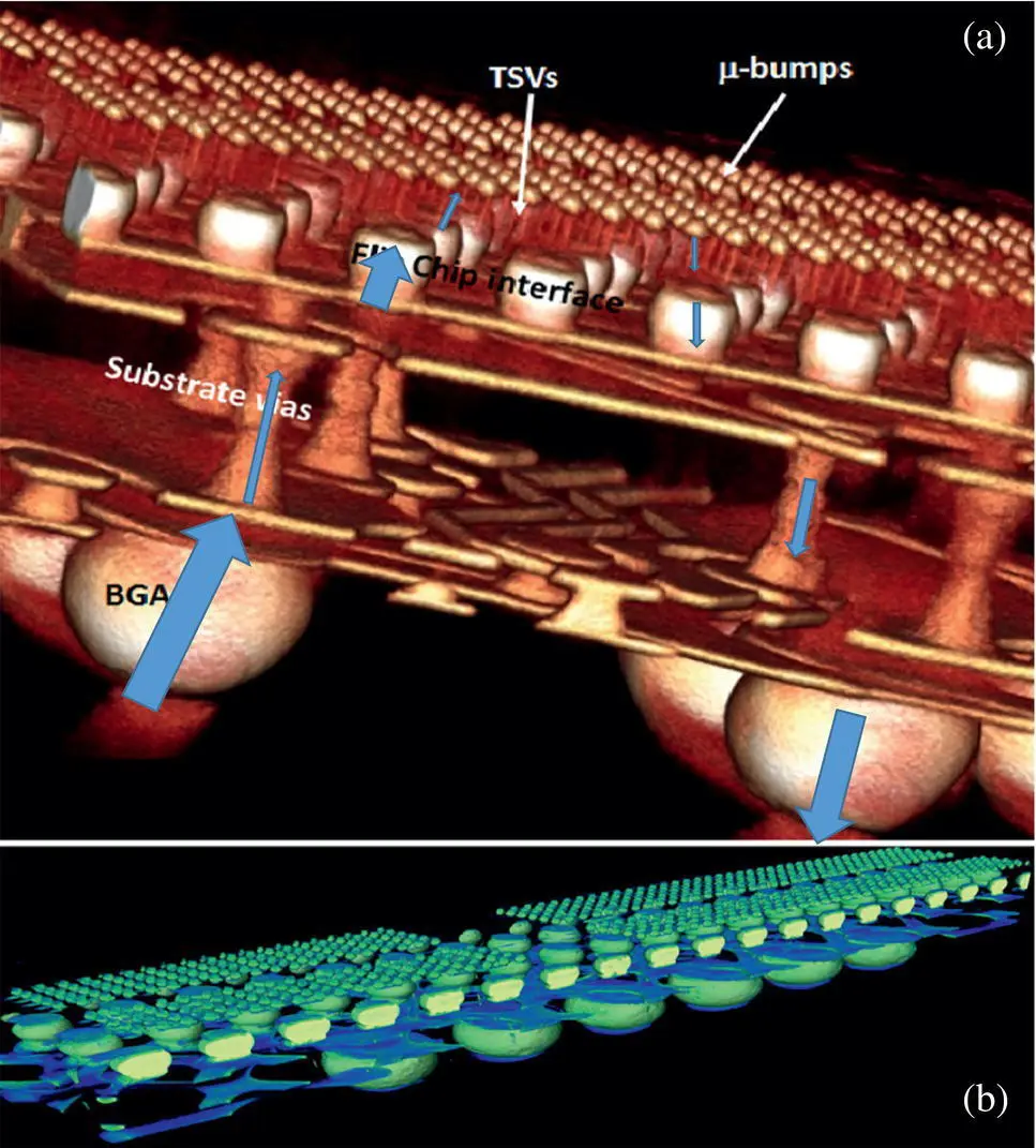
Figure 1.5 (a) Synchrotron radiation tomographic images of a similar device as shown in Figure 1.1. Due to the weak absorption of X‐ray, the two Si chips and the polymer substrate become invisible. But the solder balls and the Cu wires are shown clearly. (b) Synchrotron radiation tomographic image of a 2.5D IC device, having a length about 4 mm, and a thickness and a height of about 0.5 mm. The vertical TSV pillars can be seen.
Why do we emphasize electromigration and Joule heating? This is because electronic devices are current–voltage (I‐V) devices, so the applied electric current goes in and out of the devices in an open system. It causes Joule heating and electromigration, which are of key reliability concern. Figure 1.6is a schematic diagram of the cross‐section of a typical 3D IC device. The structure, in essence, is the same as that shown in Figure 1.4, except that on the right‐hand side, there is a stack of memory chips on a logic chip as the CPU. If we replace the stack by an optical or compound semiconductor or MEMS chip, it becomes heterogeneous integration.
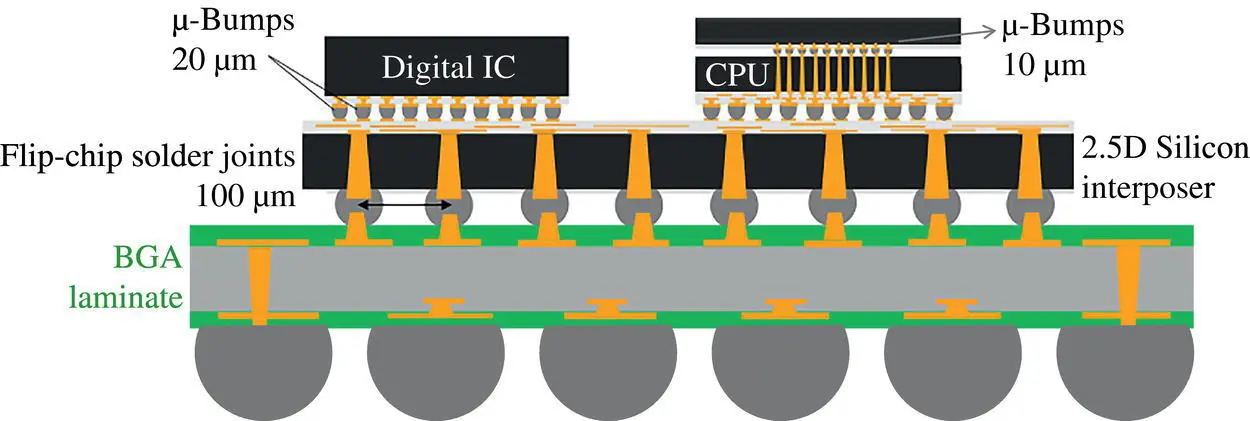
Figure 1.6 Schematic diagram of the cross‐section of a typical 3D IC device.
In comparing the structure of 3D IC to that of 2D IC, the difference is the stacking of multilayer of chips and the interconnects using TSV and μ‐bumps. On processing TSV, the thinner the chip, the easier the drilling of vias. On making μ‐bumps, its melting point should be lower than that of C‐4 joints, so that the latter will not melt upon the melting of the former. Thus, the basic challenges are that the wafer is thinner and the processing temperature is lower.
From the viewpoint of packaging technology, we may say that the essence or the major challenge in 3D IC is to scale down the dimension of packaging structures so that it can match those in the chip technology. There is no Moore’s law in packaging technology, so it has room to shrink.
What are the key functions of electronic packaging? The cell phone held in our hands is a movable electronic packaging product or a mobile computer, which enables us to compute and to communicate with the world around us. The set of chips in the cell phone can be arranged horizontally, side by side, but it takes space. Or they can be arranged vertically, one on top of the other, this is called 3D IC, and it reduces the form factor and takes less space. However, heat dissipation in 3D IC is harder because the packing is denser. When over‐heat occurs, it induces reliability problems. Over all, the product should be electrically, mechanically, chemically, and thermally stable.
1.5 Reliability Science and Engineering
An electronic device in operation is an open system because electrical charges flow in and out of the device. While the number of charges in transport is conserved, entropy production is not. The waste heat in entropy production is Joule heating on the basis of irreversible processes. [4, 5] For electrical conduction, Onsager’s Eq. ( 1.1) below shows that entropy production is the product of the conjugated flux of j (current density = coulomb/cm 2‐sec) and the conjugated driving force of E (electric field E = jρ, where ρ is resistivity). Derivation of the Onsager equation will be given in Chapter 9.
(1.1) 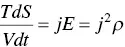
where T is the temperature, V is the volume of sample, dS/dt is the entropy production rate, and j 2 ρ is the Joule heating per unit volume per unit time. Typically, the power from Joule heating is written as P = I 2 R = j 2 ρV , where I is the applied current and R is the resistance of the sample. Thus, j 2 ρ is power density or Joule heating per unit volume per unit time of the sample, in units of Watt/cm 3, and I 2 R is Joule heating per unit time for the entire sample, in units of Watt. Clearly, this is the reason why we need low‐power devices or low entropy production devices.
While the cost of production of 3D IC can be reduced when it is in mass production, the problem of reliability due to over‐heating has to be solved fundamentally by a smart system design or by design‐for‐reliability (DfR) and by a critical selection in materials integration. To put it simply, we need to design low‐power devices, and also we need to understand heat production (Joule heating) in irreversible processes and heat dissipation in the device structure. [6] Hence, the science and engineering of electronic packaging come into focus.
Entropy production is the most relevant understanding of failure induced by electromigration, thermomigration, and stress‐migration in irreversible processes. [7] Statistical analysis of failure requires the knowing of mean‐time‐to‐failure (MTTF). An example is Black’s equation of MTTF for elctromigration. In Chapter 13, we shall present a unified model of MTTF for electromigration, thermomigration, and stress‐migration on the basis of entropy production.
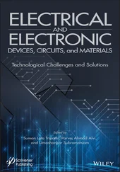
Figure 1.7shows an example of electromigration‐induced damage in Cu interconnects. The high current density in the interconnect has induced a flow of atoms along the electron flow direction, going from the cathode to the anode, leading to vacancy accumulation and void formation in the cathode region. Resistance of the interconnect increases gradually until an opening in the circuit occurs, where the resistance increases dramatically.
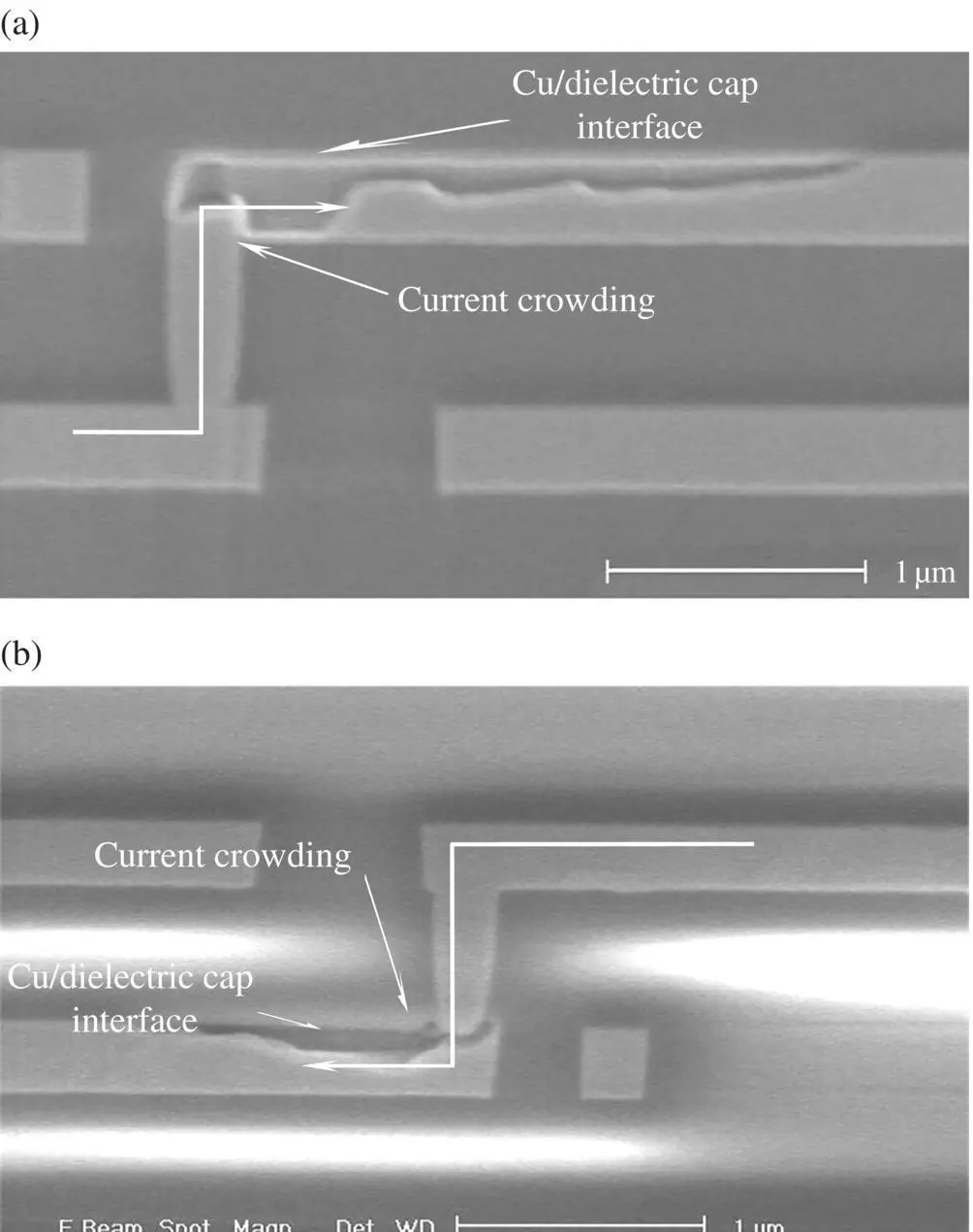
Figure 1.7 An example of electromigration electromigration‐induced failure of void formation in Cu interconnects. (a) Electrons drifted from the bottom Cu line to the top Cu line. (b) Electrons drifted from the top Cu line to the bottom Cu line.
1.6 The Future of Electronic Packaging Technology
In the near future, the R&D of packaging technology for 3D IC devices will be the focus. The role of electronic packaging in Si‐based microelectronic technology is getting more and more important. In turn, reliability will be of major concern. The introduction of AI to facilitate the applications to new 3D IC devices and the reduction of the time‐consuming reliability tests will demand our concentrated effort. In the long run, the applications of electronic packaging technology to biomedical devices will be important. For example, as people lives longer, diabetes is common in old age. To determine oxygen content and sugar content in our blood, we use invasive method to obtain a drop of blood from our finger for measurement. It is very unpleasant! If we can invent a noninvasive method, for example by wearing a mobile device around our finger or arm, it will greatly reduce the unpleasant feeling in our daily live if we have diabetes. Even better, if we can implant a small device in our body to perform the blood testing function, we will need to understand the interfacial interaction between biological and nonbiological materials. In other words, we will need to study bio‐compactable materials, as well as the chemical reactions in body fluid at body temperature. Furthermore, we may need to join a biomaterial to a non‐biomaterial. To do so, we may need a low‐temperature solder or binder which can decompose slowly in the body. However, the melting point of the common Pb‐free solder, the eutectic SnAg, is over 200 °C, to be discussed in Chapter 4on solder joint reactions. We may need a new solder whose wetting temperature is around 100 °C, which is above the working temperature and near the body temperature, for biomedical devices. While these issues are beyond the scope of this book, we note that the future of electronic packaging technology has a long way to go.
Читать дальшеИнтервал:
Закладка:
Похожие книги на «Electronic Packaging Science and Technology»
Представляем Вашему вниманию похожие книги на «Electronic Packaging Science and Technology» списком для выбора. Мы отобрали схожую по названию и смыслу литературу в надежде предоставить читателям больше вариантов отыскать новые, интересные, ещё непрочитанные произведения.


Обсуждение, отзывы о книге «Electronic Packaging Science and Technology» и просто собственные мнения читателей. Оставьте ваши комментарии, напишите, что Вы думаете о произведении, его смысле или главных героях. Укажите что конкретно понравилось, а что нет, и почему Вы так считаете.