King-Ning Tu - Electronic Packaging Science and Technology
Здесь есть возможность читать онлайн «King-Ning Tu - Electronic Packaging Science and Technology» — ознакомительный отрывок электронной книги совершенно бесплатно, а после прочтения отрывка купить полную версию. В некоторых случаях можно слушать аудио, скачать через торрент в формате fb2 и присутствует краткое содержание. Жанр: unrecognised, на английском языке. Описание произведения, (предисловие) а так же отзывы посетителей доступны на портале библиотеки ЛибКат.
- Название:Electronic Packaging Science and Technology
- Автор:
- Жанр:
- Год:неизвестен
- ISBN:нет данных
- Рейтинг книги:4 / 5. Голосов: 1
-
Избранное:Добавить в избранное
- Отзывы:
-
Ваша оценка:
Electronic Packaging Science and Technology: краткое содержание, описание и аннотация
Предлагаем к чтению аннотацию, описание, краткое содержание или предисловие (зависит от того, что написал сам автор книги «Electronic Packaging Science and Technology»). Если вы не нашли необходимую информацию о книге — напишите в комментариях, мы постараемся отыскать её.
The electronics industry is shifting towards system packaging technology due to the need for higher chip circuit density without increasing production costs. Electronic packaging, or circuit integration, is seen as a necessary strategy to achieve a performance growth of electronic circuitry in next-generation electronics. With the implementation of novel materials with specific and tunable electrical and magnetic properties, electronic packaging is highly attractive as a solution to achieve denser levels of circuit integration.
The first part of the book gives an overview of electronic packaging and provides the reader with the fundamentals of the most important packaging techniques such as wire bonding, tap automatic bonding, flip chip solder joint bonding, microbump bonding, and low temperature direct Cu-to-Cu bonding. Part two consists of concepts of electronic circuit design and its role in low power devices, biomedical devices, and circuit integration. The last part of the book contains topics based on the science of electronic packaging and the reliability of packaging technology.
Electronic Packaging Science and Technology — читать онлайн ознакомительный отрывок
Ниже представлен текст книги, разбитый по страницам. Система сохранения места последней прочитанной страницы, позволяет с удобством читать онлайн бесплатно книгу «Electronic Packaging Science and Technology», без необходимости каждый раз заново искать на чём Вы остановились. Поставьте закладку, и сможете в любой момент перейти на страницу, на которой закончили чтение.
Интервал:
Закладка:
There were many reasons of Japan’s failure, such as the critical change in currency exchange rate between yuan and dollar, and also the heavy punishments of Fujitsu by United States. However, Japan has recently joined TSMC to form an advanced electronic packaging factory in Japan to maintain its impact. The weaker and weaker presence of England and France is because of the insufficient financial support on semiconductor technology due to socialism. They tended to support rather uniformly the popular needs of society, but did not concentrate on supporting semiconductor technology. Today, to build a Si‐based transistor factory will take 3–5 billion US dollars, so fewer and fewer countries can afford it. Russia is simply poor. Samsung in Korea has had the government’s focused support to do so. TSMC in Taiwan is unique that it takes orders from all over the world to make VLSI devices, so it knows the major trend of the technology. Thus, it can spend the money it earned to keep improving the technology with innovation. For example, the technique of immersion lithography has enabled TSMC to lead the manufacturing of nanoscale semiconductor devices for the past five generations. Now, we are having the 5 nm node of nanotechnology, and 3 nm and 2 nm nodes are coming.
Some experts in China commented that China might take 10 years to catch up. No reason was given why it will take so long! On the other hand, China has been very successful in high‐speed train and satellite technology. When China can make transistors as cheap as those made in United States, it is a sign that China has caught up. A plausible reason is given below.
A Chinese classic philosopher, Wang Yang‐Ming, said “Knowing is hard, but practice is easy.” Semiconductor technology is completely opposite that “Knowing is easy, but practice is hard.” Take an example of teaching a child to play violin or piano; we can find the best teacher to teach the child all the technique and tricks of how to play well. Even a very talented child, he/she still has to take 10–20 years of practice to be good. It is the “experience” that is needed to do well. Indeed, “experience” cannot be taught quickly and cannot be copied or cannot be steal. Furthermore, in semiconductor manufacturing, the experience is not just of one person, it is of an entire industry.
1.2 Impact of Moore’s Law on Si Technology
Moore’s law states that the transistor density per chip area is doubling every 18–24 months without the increase of production cost. Figure 1.1depicts the achievements of 2D IC of Si technology according to Moore’s law. From 1970 to 1985, the density has increased from 1K to 1M per chip, which is an increase of 1000 times. From 1985 to 2005, the increase was from 1M to 1G, which is another increase of 1000 times. It is the most successful event of sustainability for about 40 years of any human activity.
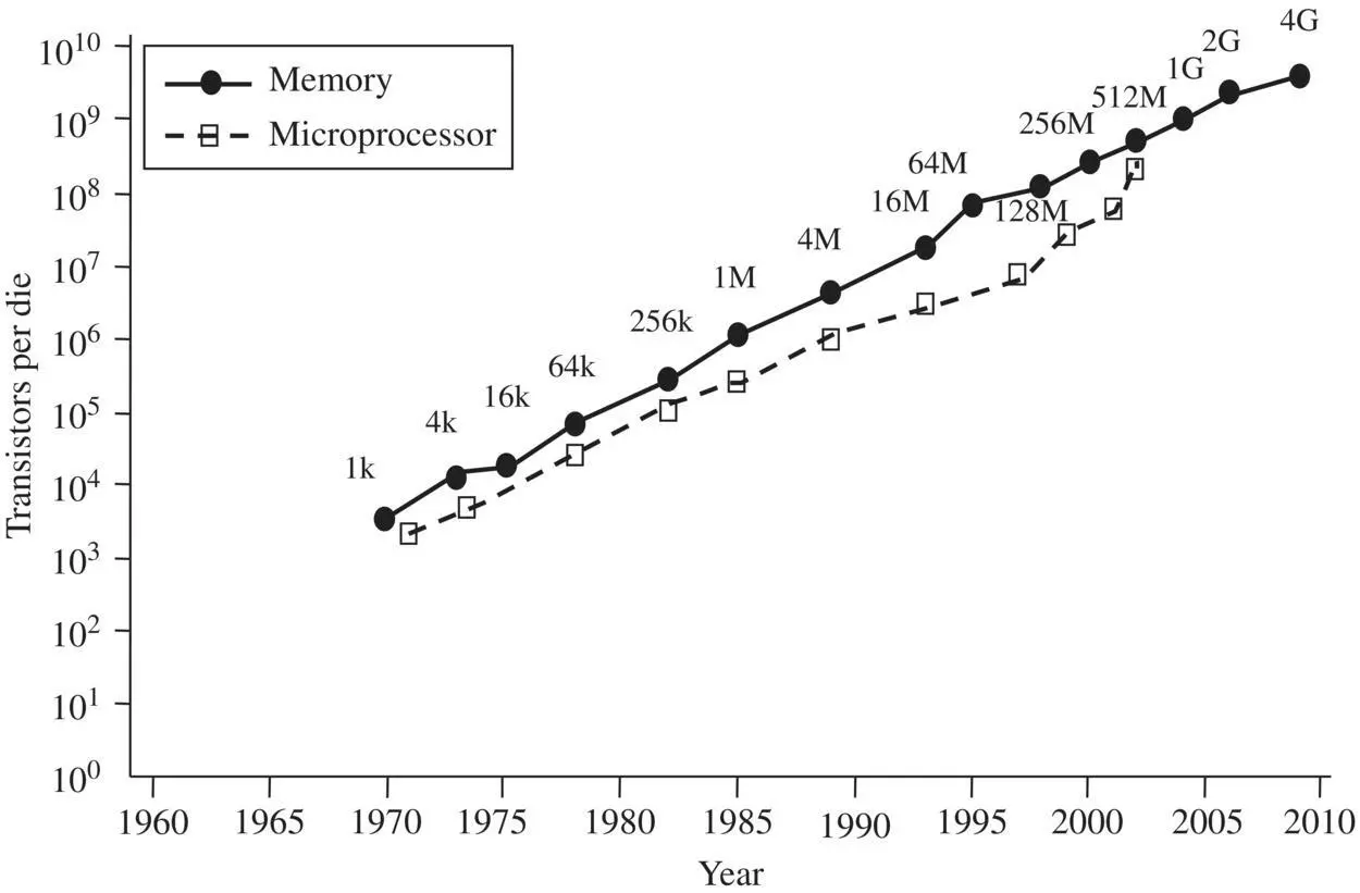
Figure 1.1 A sketch of the achievements of 2D IC of Si technology according to Moore’s law.
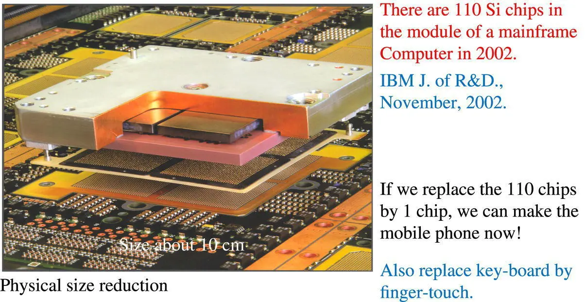
Figure 1.2 An image of part of the device structure of the mainframe computer in 2002. The size of the module is about 10 × 10 cm.
The law has had two significant impacts. First, the price of one transistor is now cheaper than the printing of one alphabet on a newspaper, which is a significant consequence of the Moore’s law that circuit density can be doubled without the increase of production cost. Hence, we can have very low cost use of transistors. Second, it enables the reduction of physical size of a computer so that handheld and mobile devices can be made. Figure 1.2shows part of a mainframe computer in 2002. The module size is about 10 × 10 cm, and between two of the ceramic plates in the module, there are 10 × 11 = 110 pieces of Si chips. According to Moore’s law shown in Figure 1.1, the circuit density per chip in 2002 is about 256 M. If we can integrate the central processing unit (CPU) and the memory on the 110 chips into a single chip, we can build a mobile device or a mobile computer by using a single chip! No doubt, we also need to reduce the packaging structure, as well as to replace a keyboard by the finger‐touching technique. It is worth mentioning that in Figure 1.2, while we do not see the chips but we see the electronic packaging structure, wherein the bright solder joints are everywhere. It shows how important is solder joint technology in electronic device manufacturing. This is because solder joint is still the best way to join two Cu wires, even two nanowires of Cu.
1.3 5G Technology and AI Applications
Those advances mentioned in the above have changed internet to mobile internet. Internet means computer‐to‐computer communication. Mobile internet means mobile computer (cell phone)‐to‐mobile computer communication. At this moment, the rapid advances in 5G and AI require Moore’s law to keep going ahead for at the least another 10–20 years, but Moore’s law is ending.
In human civilization, the technique of communication has advanced step‐by‐step slowly from language, written words, printing, telephone and telegraph, television, internet, and now to mobile internet. Today, the advanced communication technology behind mobile internet is defined as 5G, with a standard of certain required performance. Figure 1.3shows the drawing of a flower, which has six petals. There are two sets of petals: the inner brighter ones and the outer darker ones. The latter represents 5G technology and the former represents 4G technology. Each petal defines a specific technical requirement, as shown in Table 1.1. For example, on point‐to‐point latency of signals, it was 10 ms in 4G and about 1 ms in 5G. If we can advance the required performance beyond the petals of 5G, it will be 6G.
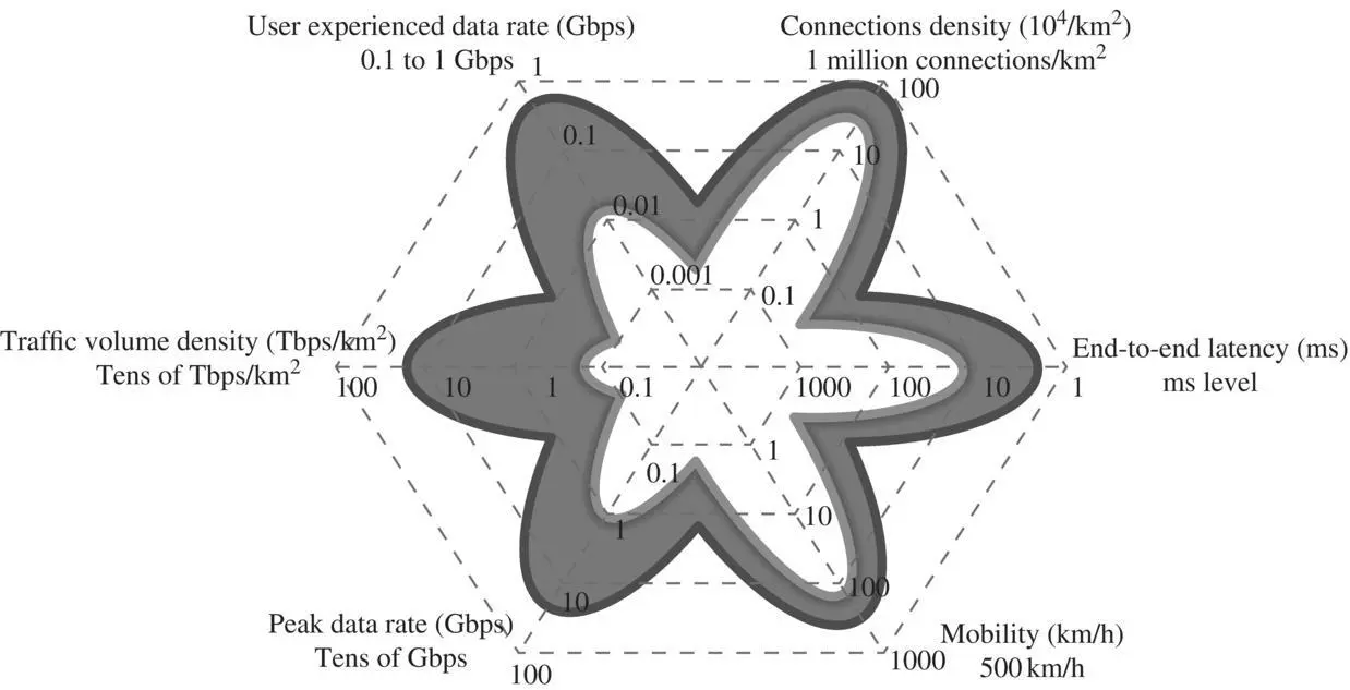
Figure 1.3 The petals of flower, which shows the required functions in 4G and 5G communication technology.
Table 1.1 5G technical requirements.
| Primary requirements:End‐to‐end latency (mille sec)Peak data rate (mobility, km/h)Traffic volume density (tens of Tbps/km 2)Density of base stations (10 4/km 2)Internet of everythingEnergy efficiency |
| Secondary requirements:Security and reliabilityLow cost |
In 2014, it was already predicted that around 2020, the 5G technology will be widely available. However, the company, Huawei in China, announced that its 5G technology is ready in 2019, ahead of everyone. It became a critical issue in the trade war between China and United States. The latter has put Huawei on its entity list or ban list. The hardware in 5G consists of satellites, servers, optical fiber lines, base stations, cell phones, and terminal sensors, and the software consists of various mobile internets, such as Android of Google. Huawei is especially good at making base stations.
Data and signals can be transmitted via satellites in sky, but satellites can be shot down easily in the beginning of a war. It can be transmitted via optical fibers underground and across oceans. The making of optical fiber requires the doping of rare‐earth elements, so the strategic importance of rare‐earth elements can be appreciated. Also it can be transmitted via base stations on land surface, so the construction of a large number of base stations is of national security concern. It is worth mentioning that Taiwan has successfully used its network of base stations to detect and control the motion and contact of people with Covid virus.
Читать дальшеИнтервал:
Закладка:
Похожие книги на «Electronic Packaging Science and Technology»
Представляем Вашему вниманию похожие книги на «Electronic Packaging Science and Technology» списком для выбора. Мы отобрали схожую по названию и смыслу литературу в надежде предоставить читателям больше вариантов отыскать новые, интересные, ещё непрочитанные произведения.


Обсуждение, отзывы о книге «Electronic Packaging Science and Technology» и просто собственные мнения читателей. Оставьте ваши комментарии, напишите, что Вы думаете о произведении, его смысле или главных героях. Укажите что конкретно понравилось, а что нет, и почему Вы так считаете.