Ernst Lueder - Liquid Crystal Displays
Здесь есть возможность читать онлайн «Ernst Lueder - Liquid Crystal Displays» — ознакомительный отрывок электронной книги совершенно бесплатно, а после прочтения отрывка купить полную версию. В некоторых случаях можно слушать аудио, скачать через торрент в формате fb2 и присутствует краткое содержание. Жанр: unrecognised, на английском языке. Описание произведения, (предисловие) а так же отзывы посетителей доступны на портале библиотеки ЛибКат.
- Название:Liquid Crystal Displays
- Автор:
- Жанр:
- Год:неизвестен
- ISBN:нет данных
- Рейтинг книги:4 / 5. Голосов: 1
-
Избранное:Добавить в избранное
- Отзывы:
-
Ваша оценка:
Liquid Crystal Displays: краткое содержание, описание и аннотация
Предлагаем к чтению аннотацию, описание, краткое содержание или предисловие (зависит от того, что написал сам автор книги «Liquid Crystal Displays»). Если вы не нашли необходимую информацию о книге — напишите в комментариях, мы постараемся отыскать её.
THE NEW EDITION OF THE GOLD-STANDARD IN TEACHING AND REFERENCING THE FUNDAMENTALS OF LCD TECHNOLOGIES
Liquid Crystal Displays — читать онлайн ознакомительный отрывок
Ниже представлен текст книги, разбитый по страницам. Система сохранения места последней прочитанной страницы, позволяет с удобством читать онлайн бесплатно книгу «Liquid Crystal Displays», без необходимости каждый раз заново искать на чём Вы остановились. Поставьте закладку, и сможете в любой момент перейти на страницу, на которой закончили чтение.
Интервал:
Закладка:
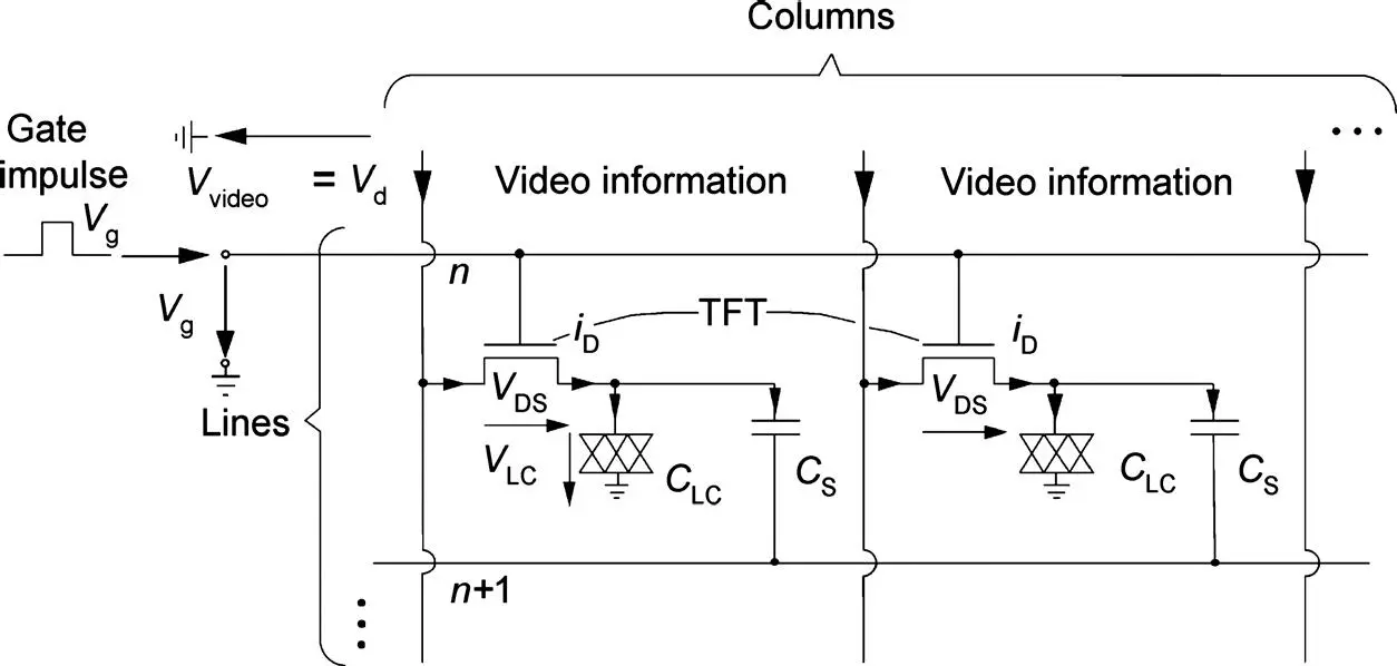
Figure 2.16 TFT addressing of the pixels in a row
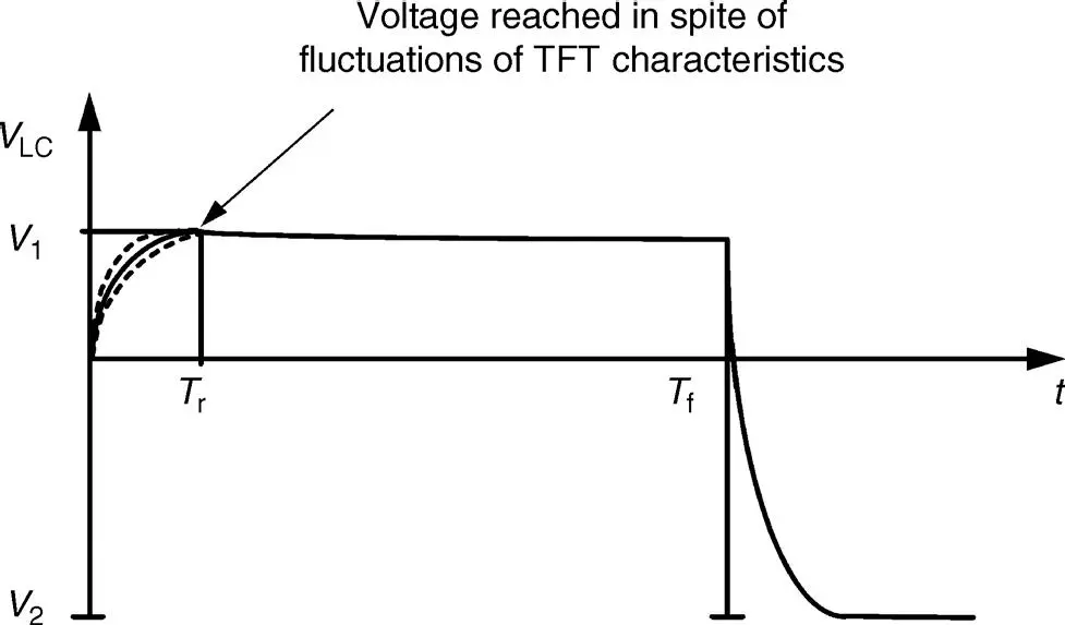
Figure 2.17 Waveform of the voltage across a pixel during charging and discharge of the storage capacitor
(2.19) 
which ensures a voltage drop of only 1 percent at T f. From Equations (2.18)and (2.19), we obtain
(2.20) 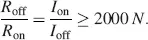
For an NTSC display with N= 484, we require R off/ R on≥ 968 × 10 3. With the practically achievable value for the off-current I off = 1 pA, the value for the on-current I on≥ 1 μ A meets the constraint in inequality (2.20).
The voltage across the pixels has to be free of dc in order to avoid dissociation of the ingredients in the LC material. Therefore, the voltage V LCapplied in the next frame time has the alternate sign as indicated in Figure 2.17. As we have observed in Section 2.2.1, the operation of the TN cell is independent of the sign of the electrical field vector. The alteration in sign from frame to frame is mandatory for a sufficient life of the LC cell. The transmitted luminance of an LC cell in Figure 2.13exhibits a linear dependence on V LCin a range of about 3 V. For 256 grey shades, this results in steps of 11.7 mV/grey shade. Special care will be taken to ensure the accuracy of these steps, as the voltages are altered by parasitic capacitive couplings. Remedies against this damage will be the alternating signs of V LCfrom row to row, column to column, frame to frame, and combinations of these measures.
TFT-addressed LCDs offer an appealing picture quality, mainly due to the absence of flicker. TFTs are fabricated together with the storage capacitors, ITO electrodes and conductors in thin film technology on glass or plastics as substrates. Glass substrates used to be 1.2 mm thick, and are presently down to 0.7 mm, whereas plastic materials excel in a thickness of only 100 μ to 200 μ. As monocrystalline layers are unfeasible in thin film technology, the semiconductor in the TFTs is either amorphous or polycrystalline. Materials are a-Si, poly-Si and, more seldom, CdSe. Alternative pixel switches are MIMs or thin film diodes.
A more economical method of addressing does not require the above-mentioned pixel switches, and generates the voltages across the pixels by a superposition of voltages at the contact pads. This is called Passive Matrix (PM) addressing which, however, exhibits shortcomings.
A more detailed discussion of all addressing schemes starts with Chapter 10.
References
1 Bahadur, B. (1990) Liquid Crystals, Applications and Uses, vol. 1. World Scientific.
2 Born, M. and Wolf, E. (1980) Principles of Optics, 6th ed., Pergamon Press, Oxford.
3 Demus, D., Goodby, J., Gray, G. W., Spiess, H.-W. and Vill, V. (1998a) Handbook of Liquid Crystals, vol. 2A. Wiley-VCH.
4 Demus, D., Goodby, J., Gray, G. W., Spiess, H.-W. and Vill, V. (1998b) Handbook of Liquid Crystals, vol. 2B. Wiley-VCH.
5 Kaneko, E. (1987) Liquid Crystal TV Displays. KTK Scientific Publishers, Tokyo.
6 Lueder, E. (1998a) Fundamentals of Passive and Active Matrix Liquid Crystal Displays. Short Course S-1, SID, May.
7 Tsvetkov, V. (1942) Acta Physicochim. (USSR) 16, 132.
3
Electro-optic Effects in Untwisted Nematic Liquid Crystals
3.1 The Planar and Harmonic Wave of Light
A planar and harmonic wave of light (Lueder, 1998a; Born and Wolf, 1980; Yeh, 1988) is assumed to propagate through anisotropic liquid crystal layers with refractive indices n ||and n┴ . Together with a polarizer and an analyser, they generate grey shades controlled by a voltage. For the derivation of these electro-optic effects, we first need to consider the basic equations for planar harmonic waves. A harmonic electric field E ( t ) with amplitude E 0is given by the scalar
(3.1) 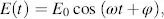
where t is the time, ω the angular frequency and φ a phase angle. A travelling planar wave is a harmonic oscillation in a plane A in Figure 3.1in the distance 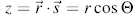 propagating in the direction of the unit vector
  with the speed
  is the vector from the origin to any location in the plane. Hence, replacing t by
  yields the equation for the planar harmonic wave in space and time as
(3.2) 
Maxwell’s equations provide for the speed of light in vacuum
(3.3) 
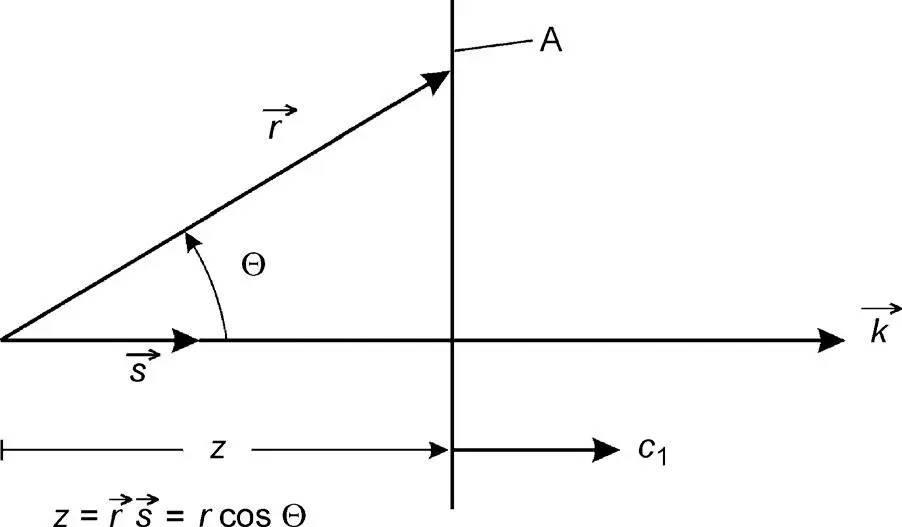
Figure 3.1 The plane A in which a planar wave travels with speed c 1and wave vector  parallel to the normal
and in materials
(3.4) 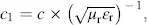
where μ 0, ε 0are the permeability and permittivity in vacuum, and μ rand ε rare the pertinent relative constants in materials. Further, for μ r= 1 the refractive index is 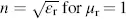 , as known from Equation (2.6).
The wavelength λ in vacuum is given by
(3.5) 
where f= ω/2π is the frequency. Equations (3.4), (2.6)and (3.5)provide for μ r=1:
Читать дальшеИнтервал:
Закладка:
Похожие книги на «Liquid Crystal Displays»
Представляем Вашему вниманию похожие книги на «Liquid Crystal Displays» списком для выбора. Мы отобрали схожую по названию и смыслу литературу в надежде предоставить читателям больше вариантов отыскать новые, интересные, ещё непрочитанные произведения.


Обсуждение, отзывы о книге «Liquid Crystal Displays» и просто собственные мнения читателей. Оставьте ваши комментарии, напишите, что Вы думаете о произведении, его смысле или главных героях. Укажите что конкретно понравилось, а что нет, и почему Вы так считаете.