Savo G. Glisic - Artificial Intelligence and Quantum Computing for Advanced Wireless Networks
Здесь есть возможность читать онлайн «Savo G. Glisic - Artificial Intelligence and Quantum Computing for Advanced Wireless Networks» — ознакомительный отрывок электронной книги совершенно бесплатно, а после прочтения отрывка купить полную версию. В некоторых случаях можно слушать аудио, скачать через торрент в формате fb2 и присутствует краткое содержание. Жанр: unrecognised, на английском языке. Описание произведения, (предисловие) а так же отзывы посетителей доступны на портале библиотеки ЛибКат.

- Название:Artificial Intelligence and Quantum Computing for Advanced Wireless Networks
- Автор:
- Жанр:
- Год:неизвестен
- ISBN:нет данных
- Рейтинг книги:3 / 5. Голосов: 1
-
Избранное:Добавить в избранное
- Отзывы:
-
Ваша оценка:
Artificial Intelligence and Quantum Computing for Advanced Wireless Networks: краткое содержание, описание и аннотация
Предлагаем к чтению аннотацию, описание, краткое содержание или предисловие (зависит от того, что написал сам автор книги «Artificial Intelligence and Quantum Computing for Advanced Wireless Networks»). Если вы не нашли необходимую информацию о книге — напишите в комментариях, мы постараемся отыскать её.
A practical overview of the implementation of artificial intelligence and quantum computing technology in large-scale communication networks Artificial Intelligence and Quantum Computing for Advanced Wireless Networks
Artificial Intelligence and Quantum Computing for Advanced Wireless Networks
Artificial Intelligence and Quantum Computing for Advanced Wireless Networks — читать онлайн ознакомительный отрывок
Ниже представлен текст книги, разбитый по страницам. Система сохранения места последней прочитанной страницы, позволяет с удобством читать онлайн бесплатно книгу «Artificial Intelligence and Quantum Computing for Advanced Wireless Networks», без необходимости каждый раз заново искать на чём Вы остановились. Поставьте закладку, и сможете в любой момент перейти на страницу, на которой закончили чтение.
Интервал:
Закладка:
3.5 Cellular Neural Networks (CeNN)
A spatially invariant CeNN architecture [14, 15] is an M × N array of identical cells ( Figure 3.21[top]). Each cell, C ij, ( i , j ) ∈ {1, M } × {1, N }, has identical connections with adjacent cells in a predefined neighborhood, N r( i , j ), of radius r . The size of the neighborhood is m = (2 r + 1) 2, where r is a positive integer.
A conventional analog CeNN cell consists of one resistor, one capacitor, 2 m linear voltage‐controlled current sources (VCCSs), one fixed current source, and one specific type of nonlinear voltage‐controlled voltage source ( Figure 3.21[bottom]). The input, state, and output of a given cell C ijcorrespond to the nodal voltages u ij, x ij, and y ijrespectively. VCCSs controlled by the input and output voltages of each neighbor deliver feedback and feedforward currents to a given cell. The dynamics of a CeNN are captured by a system of M × N ordinary differential equations, each of which is simply the Kirchhoff’s current law (KCL) at the state nodes of the corresponding cells per Eq. (3.74).
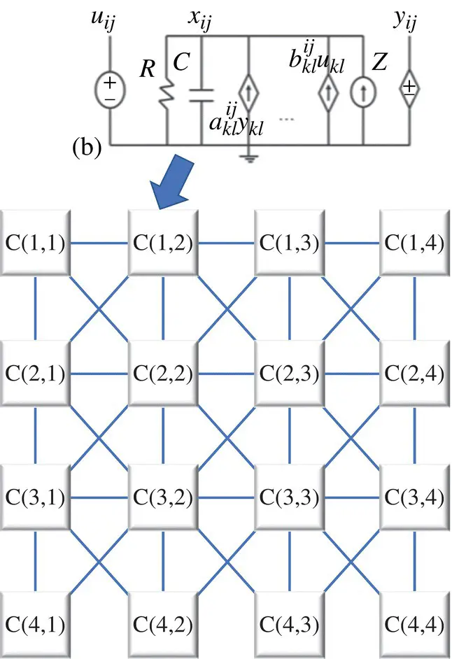
Figure 3.21 (Top) Cellular neural networks (CeNN) architecture, (bottom) circuitry in CeNN cell.
(3.74) 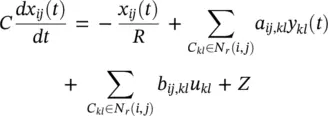
CeNN cells typically employ a nonlinear sigmoid‐like transfer function at the output to ensure fixed binary output levels. The parameters a ij,kland b ij,klserve as weights for the feedback and feedforward currents from cell C klto cell C ij. Parameters a ij,kland b ij,klare space invariant and are denoted by two (2 r + 1) × (2 r + 1) matrices. (If r = 1, they are captured by 3 × 3 matrices.) The matrices of a and b parameters are typically referred to as the feedback template ( A ) and the feedforward template ( B ), respectively. Design flexibility is further enhanced by the fixed bias current Z that provides a means to adjust the total current flowing into a cell. A CeNN can solve a wide range of image processing problems by carefully selecting the values of the A and B templates (as well as Z ). Various circuits, including inverters, Gilbert multipliers, operational transconductance amplifiers (OTAs), etc. [15, 16], can be used to realize VCCSs. OTAs provide a large linear range for voltage‐to‐current conversion, and can implement a wide range of transconductances allowing for different CeNN templates. Nonlinear templates/OTAs can lead to CeNNs with richer functionality. For more information, see [14,17–19].
Memristor‐based cellular nonlinear/neural network (MCeNN): The memristor was theoretically defined in the late 1970s, but it garnered renewed research interest due to the recent much‐acclaimed discovery of nanocrossbar memories by engineers at the Hewlett‐Packard Labs. The memristor is a nonlinear passive device with variable resistance states. It is mathematically defined by its constitutive relationship of the charge q and the flux ϕ , that is, dϕ/dt = (dϕ(q)/dq)·dq/dt . Based on the basic circuit law, this leads to v(t) = (dϕ(q)/dq)·i(t) = M(q)i(t) , where M(q) is defined as the resistance of a memristor, called the memristance , which is a function of the internal current i and the state variable x . The Simmons tunnel barrier model is the most accurate physical model of TiO 2/TiO 2−xmemristor, reported by Hewlett‐Packard Labs [20].
The memristor is expected to be co‐integrated with nanoscale CMOS technology to revolutionize conventional von Neumann as well as neuromorphic computing. In Figure 3.22, a compact convolutional neural network (CNN) model based on memristors is presented along with its performance analysis and applications. In the new CNN design, the memristor bridge circuit acts as the synaptic circuit element and substitutes the complex multiplication circuit used in traditional CNN architectures. In addition, the negative differential resistance and nonlinear current–voltage characteristics of the memristor have been leveraged to replace the linear resistor in conventional CNNs. The proposed CNN design [21–26] has several merits, for example, high density, nonvolatility, and programmability of synaptic weights. The proposed memristor‐based CNN design operations for implementing several image processing functions are illustrated through simulation and contrasted with conventional CNNs.
Training MCeNN: In the classical representation, the conductance of a memristor G depends directly on the integral over time of the voltage across the device, sometimes referred to as the flux. Formally, a memristor obeys i ( t ) = G ( s ( t ))v( t ) and  . A generalization of the memristor model, called a memristive system , was proposed in [27]. In memristive devices, s is a general state variable, rather than an integral of the voltage. Such memristive models, which are more commonly used to model actual physical devices, are discussed in [20, 28, 29]. For simplicity, we assume that the variations in the value of s ( t ) are restricted to be small so that G ( s ( t )) can be linearized around some point s *, and the conductivity of the memristor is given, to first order, by
 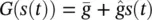 , where
 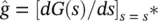 and
and 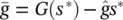 . Such a linearization is formally justified if sufficiently small inputs are used, so that s does not stray far from the fixed point (i.e.
  , making second‐order contributions negligible). The only (rather mild) assumption is that G ( s ) is differentiable near s *. Despite this linearization, the memristor is still a nonlinear component, since from the previous relations we have
 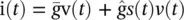 . Importantly, this nonlinear product s ( t ) v ( t ) underscores the key role of the memristor in the proposed design, where an input signal v( t ) is being multiplied by an adjustable internal value s( t ). Thus, the memristor enables an efficient implementation of trainable multilayered neural networks (MNNs) in hardware, as explained below.
Интервал:
Закладка:
Похожие книги на «Artificial Intelligence and Quantum Computing for Advanced Wireless Networks»
Представляем Вашему вниманию похожие книги на «Artificial Intelligence and Quantum Computing for Advanced Wireless Networks» списком для выбора. Мы отобрали схожую по названию и смыслу литературу в надежде предоставить читателям больше вариантов отыскать новые, интересные, ещё непрочитанные произведения.


Обсуждение, отзывы о книге «Artificial Intelligence and Quantum Computing for Advanced Wireless Networks» и просто собственные мнения читателей. Оставьте ваши комментарии, напишите, что Вы думаете о произведении, его смысле или главных героях. Укажите что конкретно понравилось, а что нет, и почему Вы так считаете.