Ibrahim Dogan - Advanced PIC Microcontroller Projects in C
Здесь есть возможность читать онлайн «Ibrahim Dogan - Advanced PIC Microcontroller Projects in C» весь текст электронной книги совершенно бесплатно (целиком полную версию без сокращений). В некоторых случаях можно слушать аудио, скачать через торрент в формате fb2 и присутствует краткое содержание. Город: Burlington, Год выпуска: 2008, ISBN: 2008, Издательство: Elsevier Ltd, Жанр: Программирование, Компьютерное железо, на английском языке. Описание произведения, (предисловие) а так же отзывы посетителей доступны на портале библиотеки ЛибКат.
- Название:Advanced PIC Microcontroller Projects in C
- Автор:
- Издательство:Elsevier Ltd
- Жанр:
- Год:2008
- Город:Burlington
- ISBN:978-0-7506-8611-2
- Рейтинг книги:5 / 5. Голосов: 1
-
Избранное:Добавить в избранное
- Отзывы:
-
Ваша оценка:
Advanced PIC Microcontroller Projects in C: краткое содержание, описание и аннотация
Предлагаем к чтению аннотацию, описание, краткое содержание или предисловие (зависит от того, что написал сам автор книги «Advanced PIC Microcontroller Projects in C»). Если вы не нашли необходимую информацию о книге — напишите в комментариях, мы постараемся отыскать её.
• Features 20 complete, tried and test projects
• Includes a CD-ROM of all the programs, hex listings, diagrams, and data sheets
Advanced PIC Microcontroller Projects in C — читать онлайн бесплатно полную книгу (весь текст) целиком
Ниже представлен текст книги, разбитый по страницам. Система сохранения места последней прочитанной страницы, позволяет с удобством читать онлайн бесплатно книгу «Advanced PIC Microcontroller Projects in C», без необходимости каждый раз заново искать на чём Вы остановились. Поставьте закладку, и сможете в любой момент перейти на страницу, на которой закончили чтение.
Интервал:
Закладка:
Table 7.4: Structure of the CSD register
| Bytes | |
|---|---|
| Byte 0 | 0 0 XXXXXX |
| Byte 1 | TAAC [7:0] |
| Byte 2 | NSAC [7:0] |
| Byte 3 | TRAN_SPEED [7:0] |
| Byte 4 | CCC [11:4] |
| Byte 5 | CCC [3:0] READ_BL_LEN [3:0] |
| Byte 6 | READ_BL_PARTIAL WRITE_BLK_MISALIGN READ_BLK_MISALIGN DSR_IMP X X C_SIZE (11:10) |
| Byte 7 | C_SIZE [9:2] |
| Byte 8 | C_SIZE [1:0] VDD_R_CURR_MIN (2:0) VDD_R_CURR_MAX (2:0) |
| Byte 9 | VDD_W_CURR_MIN (2:0) VDD_W_CURR_MAX (2:0) C_SIZE_MULT (2:1) |
| Byte 10 | ERASE_BLK_EN SECTOR_SIZE (6:1) |
| Byte 11 | SECTOR_SIZE (0) WP_GRP_SIZE (6:0) |
| Byte 12 | WP_GRP_ENABLE X X R2W_FACTOR(2:0) |
| Byte 13 | WRITE_BL_LEN (1:0) 0 X X X X X |
| Byte 14 | FILE_FORMAT_GRP COPY PERM_WRITE_PROTECT TMP_WRITE_PROTECT FILE_FORMAT (1:0) X X |
| Byte 15 | CRC (6:0) 1 |
| Field definitions | |
|---|---|
| TAAC | data read access time 1 (e.g., 1.5ms) |
| NSAC | data read access time in CLK cycles |
| TRAN_SPEED | max data transfer rate |
| CCC | card command classes |
| READ_BL_LEN | max read data block length (e.g., 512 bytes) |
| READ_BL_PARTIAL | partial blocks for read allowed |
| WRITE_BLK_MISALIGN | write block misalignment |
| READ_BLK_MISALIGN | read block misalignment |
| DSR_IMP DSR | implemented |
| C_SIZE | device size |
| VDD_R_CURR_MIN | max read current at VDD min |
| VDD_R_CURR_MAX | max read current at VDD max |
| VDD_W_CURR_MIN | max write current at VDD min |
| VDD_W_CURR_MAX | max write current at VDD max |
| C_SIZE_MULT | device size multiplier |
| ERASE_BLK_EN | erase single block enable |
| SECTOR_SIZE | erase sector size |
| WP_GRP_SIZE | write protect group size |
| WP_GRP_ENABLE | write protect group enable |
| R2W_FACTOR | write speed factor |
| WRITE_BL_LEN | max write data block length (e.g., 512 bytes) |
| WRITE_BL_PARTIAL | partial blocks for write allowed |
| FILE_FORMAT_GRP | file format group |
| COPY | copy flag |
| PERM_WRITE_PROTECT | permanent write protect |
| TMP_WRITE_PROTECT | temporary write protect |
| FILE_FORMAT | file format |
The SCR register is 8 bytes long and contains information about the SD card’s special features and capabilities, such as security support and data bus widths supported.
The OCR register is only 4 bytes long and stores the VDD voltage profile of the card. The OCR shows the voltage range in which the card data can be accessed.
All SD-card SPI commands are 6 bytes long, with the MSB transmitted first. Figure 7.5 shows the command format. The first byte is known as the command byte, and the remaining five bytes are called command arguments. Bit 6 of the command byte is set to 1 and the MSB bit is always 0. With the remaining six bits we have sixty-four possible commands, named CMD0 to CMD63. Some of the important commands are:
• CMD0 GO_IDLE_STATE (resets the SD card)
• CMD1 SEND_OP_COND (initializes the card)
• CMD9 SEND_CSD (gets CSD register data)
• CMD10 SEND_CID (gets CID register data)
• CMD16 SET_BLOCKLEN (selects a block length in bytes)
• CMD17 READ_SINGLE_BLOCK (reads a block of data)
• CMD24 WRITE_BLOCK (writes a block of data)
• CMD32 ERASE_WR_BLK_START_ADDR (sets the address of the first write block to be erased)
• CMD33 ERASE_WR_BLK_END_ADDR (sets the address of the last write block to be erased)
• CMD38 ERASE (erases all previously selected blocks)
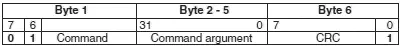
Figure 7.5: SD card SPI command format
In response to a command, the card sends a status byte known as R1. The MSB bit of this byte is always 0 and the other bits indicate the following error conditions:
• Card in idle state
• Erase reset
• Illegal command
• Communication CRC error
• Erase sequence error
• Address error
• Parameter error
The SD card in SPI mode supports single-block and multiple-block read operations. The host should set the block length. After a valid read command the card responds with a response token, followed by a data block and a CRC check. The block length can be between 1 and 512 bytes. The starting address can be any valid address in the address range of the card.
In multiple-block read operations, the card sends data blocks with each block having its own CRC check attached to the end of the block.
The SD card in SPI mode supports single-or multiple-block write operations. After receiving a valid write command from the host, the card responds with a response token and waits to receive a data block. A one-byte “start block” token is added to the beginning of every data block. After receiving the data block the card responds with a “data response” token, and the card is programmed as long as the data block is received with no errors.
In multiple-block write operations the host sends the data blocks one after the other, each preceded by a “start block” token. The card sends a response byte after receiving each data block.
Card Size Parameters SD cards are available in various sizes. At the time of writing, SanDisk Corporation (www.sandisk.com) offered the models and capacities shown in Table 7.5. The company may now be offering models with 4GB or even greater capacity.
Table 7.5: SanDisk card models and capacities
| Model | Capacities |
|---|---|
| SDSDB-16 | 16 MB |
| SDSDB-32 | 32 MB |
| SDSDJ-64 | 64 MB |
| SDSDJ-128 | 128 MB |
| SDSDJ-256 | 256 MB |
| SDSDJ-512 | 512 MB |
| SDSDJ-1024 | 1024 MB |
In addition to the normal storage area on the card, there is also a protected area pertaining to the secured copyright management. This area can be used by applications to save security-related data and can be accessed by the host using secured read/write commands. The card write protection mechanism does not affect this area. Table 7.6 shows the size of the protected area and the data area available to the user for reading and writing data. For example, a 1GB card has 20,480 blocks (one block is 512 bytes) of protected area and 1,983,744 blocks of user data area.
Table 7.6: Protected area and data area sizes
| Model | Protected area (blocks) | User area (blocks) |
|---|---|---|
| SDSDB-16 | 352 | 28,800 |
| SDSDB-32 | 736 | 59,776 |
| SDSDJ-64 | 1,376 | 121,856 |
| SDSDJ-128 | 2,624 | 246,016 |
| SDSDJ-256 | 5,376 | 494,080 |
| SDSDJ-512 | 10,240 | 940,864 |
| SDSDJ-1024 | 20,480 | 1,983,744 |
1 block = 512 bytes.
Data can be written to or read from any sector of the card using raw sector access methods. In general, SD card data is structured as a file system and two DOS-formatted partitions are placed on the card: the user area and the security protected area. The size of each area is shown in Table 7.7. For example, in a 1GB card, the size of the security protected area is 519 sectors (1 sector is 512 bytes), and the size of the user data area is 1,982,976 sectors.
Читать дальшеИнтервал:
Закладка:
Похожие книги на «Advanced PIC Microcontroller Projects in C»
Представляем Вашему вниманию похожие книги на «Advanced PIC Microcontroller Projects in C» списком для выбора. Мы отобрали схожую по названию и смыслу литературу в надежде предоставить читателям больше вариантов отыскать новые, интересные, ещё непрочитанные произведения.


Обсуждение, отзывы о книге «Advanced PIC Microcontroller Projects in C» и просто собственные мнения читателей. Оставьте ваши комментарии, напишите, что Вы думаете о произведении, его смысле или главных героях. Укажите что конкретно понравилось, а что нет, и почему Вы так считаете.