Ibrahim Dogan - Advanced PIC Microcontroller Projects in C
Здесь есть возможность читать онлайн «Ibrahim Dogan - Advanced PIC Microcontroller Projects in C» весь текст электронной книги совершенно бесплатно (целиком полную версию без сокращений). В некоторых случаях можно слушать аудио, скачать через торрент в формате fb2 и присутствует краткое содержание. Город: Burlington, Год выпуска: 2008, ISBN: 2008, Издательство: Elsevier Ltd, Жанр: Программирование, Компьютерное железо, на английском языке. Описание произведения, (предисловие) а так же отзывы посетителей доступны на портале библиотеки ЛибКат.
- Название:Advanced PIC Microcontroller Projects in C
- Автор:
- Издательство:Elsevier Ltd
- Жанр:
- Год:2008
- Город:Burlington
- ISBN:978-0-7506-8611-2
- Рейтинг книги:5 / 5. Голосов: 1
-
Избранное:Добавить в избранное
- Отзывы:
-
Ваша оценка:
Advanced PIC Microcontroller Projects in C: краткое содержание, описание и аннотация
Предлагаем к чтению аннотацию, описание, краткое содержание или предисловие (зависит от того, что написал сам автор книги «Advanced PIC Microcontroller Projects in C»). Если вы не нашли необходимую информацию о книге — напишите в комментариях, мы постараемся отыскать её.
• Features 20 complete, tried and test projects
• Includes a CD-ROM of all the programs, hex listings, diagrams, and data sheets
Advanced PIC Microcontroller Projects in C — читать онлайн бесплатно полную книгу (весь текст) целиком
Ниже представлен текст книги, разбитый по страницам. Система сохранения места последней прочитанной страницы, позволяет с удобством читать онлайн бесплатно книгу «Advanced PIC Microcontroller Projects in C», без необходимости каждый раз заново искать на чём Вы остановились. Поставьте закладку, и сможете в любой момент перейти на страницу, на которой закончили чтение.
Интервал:
Закладка:
SD card speeds are measured three different ways: in KB/s (kilobytes per second), in MB/s (megabytes per second), in an “x” rating similar to that of CD-ROMS where “x” is the speed corresponding to 150KB/s. The various “x” based speeds are:
• 4x: 600KB/s
• 16x: 2.4MB/s
• 40x: 6.0MB/s
• 66x: 10MB/s
In this chapter we are using the standard SD card only. The specifications of the smaller SD cards are the same and are not described further in this chapter.
SD cards can be interfaced to microcontrollers using two different protocols: SD card protocol and the SPI (Serial Peripheral Interface) protocol. The SPI protocol, being more widely used, is the one used in this chapter. The standard SD card has 9 pins with the pin layout shown in Figure 7.2. The pins have different functions depending on the interface protocol. Table 7.2 gives the function of each pin in both the SD and SPI modes of operation.
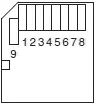
Figure 7.2: Standard SD card pin layout
Table 7.2: Standard SD card pin definitions
| Pin | Name | SD description | SPI description |
|---|---|---|---|
| 1 | CD/DAT3/CS | Data line 3 | Chip select |
| 2 | CMD/Datain | Command/response | Host to card command and data |
| 3 | VSS | Supply ground | Supply ground |
| 4 | VDD | Supply voltage | Supply voltage |
| 5 | CLK | Clock | Clock |
| 6 | VSS2 | Supply voltage ground | Supply voltage ground |
| 7 | DAT0 | Data line 0 | Card to host data and status |
| 8 | DAT1 | Data line 1 | Reserved |
| 9 | DAT2 | Data line 2 | Reserved |
Since the SD card projects described in this chapter are based on the SPI bus protocol, it is worth looking at the specifications of this bus before proceeding to the projects themselves.
7.1.1 The SPI Bus
The SPI (Serial Peripheral Interface) bus is a synchronous serial bus standard named by Motorola that operates in full duplex mode. Devices on a SPI bus operate in master-slave mode, where the master device initiates the data transfer, selects a slave, and provides a clock for the slaves. The selected slave responds and sends its data to the master at each clock pulse. The SPI bus can operate with a single master device and one or more slave devices. This simple interface is also called a “four-wire” interface.
The signals in the SPI bus are named as follows:
• MOSI — master output, slave input
• MISO — master input, slave output
• SCLK — serial clock
• SS — slave select
These signals are also named as:
• DO — data out
• DI — data in
• CLK — clock
• CD — chip select
Figure 7.3 shows the basic connection between a master device and a slave device in SPI bus. The master sends out data on line MOSI and receives data on line MISO. The slave must be selected before data transfer can take place.
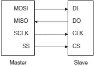
Figure 7.3: SPI master-slave connection
Figure 7.4 shows an instance where more than one slave device is connected to the SPI bus. Here, each slave is selected individually by the master, and although all the slaves receive the clock pulses, only the selected slave device responds. If an SPI device is not selected, its data output goes into a high-impedance state so it does not interfere with the currently selected device on the bus.
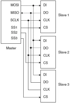
Figure 7.4: Multiple-slave SPI bus
Data transmission normally occurs in and out of the master and slave devices as the master supplies clock pulses. To begin a communication, the master first pulls the slave select line low for the desired slave device. Then the master issues clock pulses, and during each SPI clock cycle, a full duplex data transmission occurs. When there are no more data to be transmitted, the master stops toggling its clock output.
The SPI bus is currently used by microcontroller interface circuits to talk to a variety of devices such as:
• Memory devices (SD cards)
• Sensors
• Real-time clocks
• Communications devices
• Displays
The advantages of the SPI bus are:
• Simple communication protocol
• Full duplex communication
• Very simple hardware interface
Its disadvantages are:
• Requires four pins
• No hardware flow control
• No slave acknowledgment
It is worth remarking that there are no SPI standards governed by an international committee, so there are several versions of SPI bus implementation. In some applications, the MOSI and MISO lines are combined into a single data line, thereby reducing the line requirements to three. Some implementations have two clocks, one to capture (or display) data and the other to clock it into the device. Also, in some implementations the chip select line may be active-high rather than active-low.
7.1.2 Operation of the SD Card in SPI Mode
When the SD card is operated in SPI mode, only seven pins are used. Three (pins 3, 4, and 6) are used for the power supply, leaving four pins (pins 1, 2, 5, and 7) for the SPI mode of operation:
• Two power supply ground (pins 3 and 6)
• Power supply (pin 4)
• Chip select (pin 1)
• Data out (pin 7)
• Data in (pin 2)
• CLK (pin 5)
At power-up, the SD card defaults to the SD bus protocol. The card is switched to SPI mode if the Chip Select (CS) signal is asserted during reception of the reset command. When the card is in SPI mode, it only responds to SPI commands. The host may reset a card by switching the power supply off and then on again.
The mikroC compiler provides a library of commands for initializing, reading, and writing to SD cards. It is not necessary to know the internal structure of an SD card in detail before using one, since the library functions are available. However, a basic understanding of the internal structure of an SD card is helpful in making the best use of the card. In this section we will look briefly at the internal architecture and operation of SD cards.
An SD card has a set of registers that provide information about the status of the card. When the card is operated in SPI mode these are:
• Card identification register (CID)
• Card specific data register (CSD)
• SD configuration register (SCR)
• Operation control register (OCR)
The CID register consists of 16 bytes and contains the manufacturer ID, product name, product revision, card serial number, manufacturer date code, and a checksum byte. Table 7.3 shows the structure of the CID register.
Table 7.3: Structure of the CID register
| Name | Type | Width | Comments |
|---|---|---|---|
| Manufacturer ID (MID) | Binary | 1 byte | Manufacturer ID (e.g., 0x03 for SanDisk) |
| OEM/Application ID (OID) | ASCII | 2 bytes | Identifies card OEM and/or card contents |
| Product Name (PNM) | ASCII | 5 bytes | Product name |
| Product Revision (PRV) | BCD | 1 byte | Two binary coded digits |
| Serial Number (PSN) | Binary | 4 bytes | 32 bits unsigned integer |
| Reserved | 4 bits | Upper 4 bits | |
| Manufacture Date Code (MDT) | BCD | 12 bits | Manufacture date (offset from 2000) |
| CRC-7 Checksum | Binary | 7 bits | Checksum |
| Not used | Binary | 1 bit | Always 1 |
The CSD register consists of 16 bytes and contains card-specific data such as the card data transfer rate, read/write block lengths, read/write currents, erase sector size, file format, write protection flags, and checksum. Table 7.4 shows the structure of the CSD register.
Читать дальшеИнтервал:
Закладка:
Похожие книги на «Advanced PIC Microcontroller Projects in C»
Представляем Вашему вниманию похожие книги на «Advanced PIC Microcontroller Projects in C» списком для выбора. Мы отобрали схожую по названию и смыслу литературу в надежде предоставить читателям больше вариантов отыскать новые, интересные, ещё непрочитанные произведения.


Обсуждение, отзывы о книге «Advanced PIC Microcontroller Projects in C» и просто собственные мнения читателей. Оставьте ваши комментарии, напишите, что Вы думаете о произведении, его смысле или главных героях. Укажите что конкретно понравилось, а что нет, и почему Вы так считаете.