2D Monoelements
Здесь есть возможность читать онлайн «2D Monoelements» — ознакомительный отрывок электронной книги совершенно бесплатно, а после прочтения отрывка купить полную версию. В некоторых случаях можно слушать аудио, скачать через торрент в формате fb2 и присутствует краткое содержание. Жанр: unrecognised, на английском языке. Описание произведения, (предисловие) а так же отзывы посетителей доступны на портале библиотеки ЛибКат.
- Название:2D Monoelements
- Автор:
- Жанр:
- Год:неизвестен
- ISBN:нет данных
- Рейтинг книги:5 / 5. Голосов: 1
-
Избранное:Добавить в избранное
- Отзывы:
-
Ваша оценка:
2D Monoelements: краткое содержание, описание и аннотация
Предлагаем к чтению аннотацию, описание, краткое содержание или предисловие (зависит от того, что написал сам автор книги «2D Monoelements»). Если вы не нашли необходимую информацию о книге — напишите в комментариях, мы постараемся отыскать её.
Recent advances in phosphorene The diverse properties of two-dimensional antimonene, of graphene and its derivatives The molecular docking simulation study used to analyze the binding mechanisms of graphene oxide as a cancer drug carrier Metal-organic frameworks (MOFs)-derived carbon (graphene and carbon nanotubes) and MOF-carbon composite materials, with a special emphasis on the use of these nanostructures for energy storage devices (supercapacitors) Two-dimensional monoelements classification like graphene application in field-effect transistors for sensing and biosensing Graphene-based ternary materials as a supercapacitor electrode Rise of silicene and its applications in gas sensing
2D Monoelements — читать онлайн ознакомительный отрывок
Ниже представлен текст книги, разбитый по страницам. Система сохранения места последней прочитанной страницы, позволяет с удобством читать онлайн бесплатно книгу «2D Monoelements», без необходимости каждый раз заново искать на чём Вы остановились. Поставьте закладку, и сможете в любой момент перейти на страницу, на которой закончили чтение.
Интервал:
Закладка:
1.2.3.3 FETs
Another significant application of phosphorene is the fabrication of field-effect transistors (FETs) [38]. Phosphorene devices can offer many advantages over graphene transistors due to the good saturation of the current and their band gap [62]. Phosphorenes have attractive characteristics that are critical for advanced circuits and sophisticated amplifiers [10]. In particular, phosphorene exhibits drain current modulation of 10 5, high flexibility, and high carrier mobilities of about 1,000 cm 2V −1s −1which is larger than the other flexible transistors based on 2D monolayers like WSe 2and MoS 2. Furthermore, when the length of channel is 300 nm, the measurements show that phosphorene exhibits a cutoff frequency of 12 GHz for the short-circuit current while frequency oscillation reaches the value of 30 Hz.
Beyond the multi-GHz frequency, phosphorene constitutes one of the best candidates for future generations of ultrathin layer transistors [10]. Moreover, phosphorene is not only used in field-effect transistor applications, but also in other electronic devices based on semiconductor materials due to its electronic properties and its charge mobility.
1.3 Phosphorene Oxides
The non-bonding pairs of electrons present on the surface of phosphorene leads to degradation of this 2D monolayer under ambient conditions, namely, oxygen, water, and light. This impedes phosphorene from some of its potential applications. To overcome this obstacle, phosphorene oxides with different O-concentration were investigated. It follows that phosphorene is stable at low O-concentrations. More precisely, half-oxidation is the best concentration to construct a stable material.
1.3.1 Challenges: Degradation of Phosphorene
In contrast to the unique properties and great potential of phosphorene, which distinguish it from other 2D materials, phosphorene remains unstable under atmospheric conditions, for example, in the presence of oxygen, water, and light, due to the non-bonding pairs of electrons present at its surface [27, 63]. The unprotected surface of phosphorene develops significant roughness, causing important changes and consequent degradation in the compositional and physical features of the material. In some cases, the degradation poses a serious performance problem of phosphorene-based devices [64].
1.3.1.1 Light Exposure
In phosphorene, the ambient degradation in the atmosphere is divided into three stages. In the first stage, the reaction induced by the ambient light O 2leads to the formation of oxygen. In that case, the reaction expressing the transfer if charge is given by: 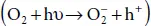 where P corresponds to phosphorene and h +is a hole with positive charge. In the second stage, the oxygen molecule is separated at the surface leading to the following:
 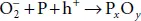 . Finally, in the last step that is a hydrogen-bond interaction, the P atom is removed from the surface and the bonded O is absorbed by water molecules. It follows that the top layer of phosphorene is broken and excitons can be produced under ambient light.
To evaluate the evolution of BP degradation for various light’s wavelengths and at different time scales, six representative BP flakes were studied individually. Using atomic force microscopy (AFM), the exposures were evaluated in a dark room at six values of wavelengths ranging from 280 to 1,050 nm and imaged before and after identical exposure durations varying from 30 to 120 min with a step of 30 min [65]. The maximum degradation was observed for the UV light (280 nm), then for the blue one (455 nm). In contrast, phosphorene does not show any degradation for green, red, and infrared light, namely, 565, 660, 850, and 1,050 nm. Consequently, the UV light is the predominant contributor to the degradation of BP.
In addition, the engineering of the phosphorene’s band gap renders this material a good candidate for a photodetector, with a large spectral response ranging from the UV towards IR region. For instance, phosphorene photon detector shows a very fast response of 1.82 A/W in the presence of visible light irradiation of 550 nm. With photon energy and a bias of 0.1 V, the photoresponsivity attains the value of 175 A/W in the NIR regime, and at a higher bias of 3 V, it reaches 9×10 4A/W offering phosphorene potential as a UV detector [66].
1.3.1.2 Phosphorene vs Air
When phosphorene is exposed directly to air, its reaction causes rapid degradation of phosphorene-based devices. Moreover, the exothermic process reveals that H 2O will react with oxidized phosphorene. Both theoretical calculations and experiments have shown that at room temperature, phosphorene undergoes a spontaneous oxidation when it is exposed to O 2. The oxidation pathway leads to the formation of phosphoric acid and defective phosphorene [29]. Besides, humidity (the presence of H 2O) is very important to determine the stability of phosphorene in air. To avoid surface degradation of phosphorene and overcoming the oxidation barrier, some passivation techniques must be introduced. For example, graphene, h-BN, AlO x , Al 2O 3, P x O y , and polymeric materials are used to protect it from mechanical and chemical degradation [28]. Under low oxidation, phosphorene is stable and tend to be less stable when increasing the oxygen concentrations [25]. Consequently, 50% oxidation of phosphorene is the best amount to stabilize phosphorene after a two-day exposure to the atmosphere [67].
1.3.1.3 Functionalized Phosphorene
Non-metallic adatoms can also be strongly bound to phosphorene due to the lone electrons pair. Functionalization of phosphorene by adsorption of non-metallic atoms with a [He] core electronic, namely, B, C, N, F, and Al showed different site preferences as schematically illustrated in Figure 1.7. Indeed, while the adatoms B, C, and Al prefer to adsorb to the hollow (H) site, F adatom is adsorbed at the top site and N adatom prefers the bridge one [68]. Furthermore, the chemical functionalization of these non-metallic adatoms exists in three classes [69]. In the first one, the C and B adatoms get located at the interstitial site after breaking the P-P bonds. However in the second group, the N and F atoms remain on the surface of the P atoms and preserve the lattice structure of phosphorene. The last group is formed by the Al impurity, located at the top of the centre of the hexagon. The interatomic distances show that the smaller the adatom, the closer it is to the P monolayer, which implies a higher binding energy compared to the larger ones. This result is confirmed by the calculations of the binding energy ( Eb ).
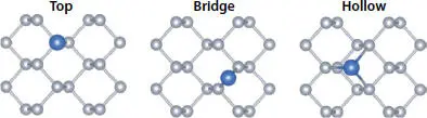
Figure 1.7 The three possible adsorption sites.
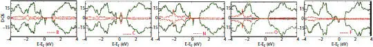
Figure 1.8 DOS of spin up and down of adatoms.
For B, C, N, F, and Al adatoms on phosphorene, Eb is −5.08, −5.16, −2.98, −2.30, and −3.18 eV, respectively [68, 70]. The adsorption process is more stable in phosphorene since the values of Eb are much greater than the case of adsorbed graphene [71–73]. The higher values of Eb are mainly deserved to the buckled sp 3configuration of the reactive material as reported in [68]. Mid-gap states are observed in the spin-polarized density of states plotted in Figure 1.8with 1 μ B for B, N, and F systems. However, the curves for the C and Al impurities reveal the same number of electrons having up-spin and down-spin, indicating the absence of magnetic order in these configurations [70].
Читать дальшеИнтервал:
Закладка:
Обсуждение, отзывы о книге «2D Monoelements» и просто собственные мнения читателей. Оставьте ваши комментарии, напишите, что Вы думаете о произведении, его смысле или главных героях. Укажите что конкретно понравилось, а что нет, и почему Вы так считаете.