2D Monoelements
Здесь есть возможность читать онлайн «2D Monoelements» — ознакомительный отрывок электронной книги совершенно бесплатно, а после прочтения отрывка купить полную версию. В некоторых случаях можно слушать аудио, скачать через торрент в формате fb2 и присутствует краткое содержание. Жанр: unrecognised, на английском языке. Описание произведения, (предисловие) а так же отзывы посетителей доступны на портале библиотеки ЛибКат.
- Название:2D Monoelements
- Автор:
- Жанр:
- Год:неизвестен
- ISBN:нет данных
- Рейтинг книги:5 / 5. Голосов: 1
-
Избранное:Добавить в избранное
- Отзывы:
-
Ваша оценка:
2D Monoelements: краткое содержание, описание и аннотация
Предлагаем к чтению аннотацию, описание, краткое содержание или предисловие (зависит от того, что написал сам автор книги «2D Monoelements»). Если вы не нашли необходимую информацию о книге — напишите в комментариях, мы постараемся отыскать её.
Recent advances in phosphorene The diverse properties of two-dimensional antimonene, of graphene and its derivatives The molecular docking simulation study used to analyze the binding mechanisms of graphene oxide as a cancer drug carrier Metal-organic frameworks (MOFs)-derived carbon (graphene and carbon nanotubes) and MOF-carbon composite materials, with a special emphasis on the use of these nanostructures for energy storage devices (supercapacitors) Two-dimensional monoelements classification like graphene application in field-effect transistors for sensing and biosensing Graphene-based ternary materials as a supercapacitor electrode Rise of silicene and its applications in gas sensing
2D Monoelements — читать онлайн ознакомительный отрывок
Ниже представлен текст книги, разбитый по страницам. Система сохранения места последней прочитанной страницы, позволяет с удобством читать онлайн бесплатно книгу «2D Monoelements», без необходимости каждый раз заново искать на чём Вы остановились. Поставьте закладку, и сможете в любой момент перейти на страницу, на которой закончили чтение.
Интервал:
Закладка:
Furthermore, the puckered structure of phosphorene attributes its interesting elastic properties such as great structural flexibility and a resistance to 27% and 30% deformations along the zigzag and armchair directions, respectively [22, 23], which makes this material very suitable for wearable optoelectronic devices. Furthermore, the Young’s modulus and Poisson ratio exhibit their maximum values along ZZ-axis indicating how it is difficult to strain it. Consequently, phosphorene is super flexible along the armchair axis [23]. It is also well to mention that phosphorene is an auxetic material [24, 25] and that its non-centrosymmetric point group leads to a large piezoelectric response [23] showing that phosphorene can convert mechanical energy into electrical one [26].
Despite all the exceptional properties of phosphorene, it is very reactive with oxygen due to the non-bonding pairs present at its surface [27]. This fact limits its applications in optoelectronics, sensors, energy conversion, photocatalytic, and so on. To overcome this obstacle, many different techniques have been used to fabricate air-stable phosphorene. The passivated phosphorene by graphene, h-BN, Al 2O 3, and the polymeric material is a promising technique to avoid chemical debasement and to modulate its features [28]. The measurements shown smaller degradation when phosphorene only exposes to O 2or H 2 O [29]. Phosphorene with different oxygen concentrations confers excellent new properties in these 2D materials [30, 31]. At high concentration, oxidation leads to a new family, namely, 2D planar and 1D tubular forms, with a transition in the band gap from semiconductors to insulators [32].
In this chapter, we first present pure phosphorene starting from its crystalline structures, its fabrication methods, its physical properties, and ending with certain applications. Secondly, we will investigate how the oxidation’s arrangement and concentrations influence the electronic, elastic, and optical characteristics of phosphorene oxides.
1.2 Pristine 2D BP
Owing to its great buckle height, phosphorene has fascinating properties such as anisotropic optoelectronic and mechanical features which make it very attractive for nanodevices.
1.2.1 Synthesis and Characterization
Similar to graphene, 2D BP can be exfoliated from buckled material trough the top down method. The bottom-up method is still not promising for phosphorene CVD growth since most of the phosphorus precursors used in thermal depositions show a high amount of toxicity and cannot be adapted for CVD manufactures [33, 34]. It follows that the large-scale bottom-up method requires more effort from experimental scientists.
1.2.1.1 Top-Down Approaches
The mechanical exfoliation is an effective widely used method for cleaving 3D materials from mutilayers to some layers and then to isolate a single layer [34]. Graphene monolayer, for example, has been isolated from graphite simply by using adhesive tape [35, 36].
Monolayer, bi- and tri-BP sheets were successfully exfoliated using micromechanical cleavage of 3D BP with PDMS in 2014. This method was carried out using an adhesive tape in three steps.
First, the exfoliated phosphorene layers were transferred to PMMA/PVA (polymethyl methacrylate/Polyvinyl Alcohol) composites, and then, the resulting layers with the composites were moved to a SiN substrate with a thickness of 200 nm. Several chemicals are used to separate the obtained specimens from the PMMA/PVA composites and to ensure that no more scotch tapes was left [37]. Despite the success of the mechanical exfoliation process, it was found that it was not scalable and hence limited to be used in academic laboratories for fundamental studies. Thus, to obtain a phosphorene sheet, a more efficient manufacturing process has been introduced. In particular, an Ar+ plasma was used to produce monolayer phosphorene through thermal ablation. This process provides an improved means of controlling the phosphorene thickness, unlike it is still challenging for mass production [38, 39].
The interesting technique to fabricate large quantities of exfoliated phosphorene is the liquid phase preparation. The solution-based phosphorene synthesis is placed into the BP interlayers which enlarge the distance and allows the exfoliation. This approach is widely used to manufacture several 2D and 3D materials that have shown good performance in dispositive [40].
1.2.1.2 Bottom-Up Methods
Advanced chemical techniques were used intensively to fabricate large quantities of innovative devices based on new 2D sheets like graphene, germanene, borophene, silicene, and stanene [38]. For other synthesized 2D materials, this new processing route based on the deposition via thermal evaporation of their elemental forms is done on available suitable substrates/surfaces like Ag(111), Au(111), Pt(111), and Al(111) [34]. In parallel, other means, such as the successful epitaxial growth of graphene and TMDCs on insulating substrates made of sapphire or 300 nm of SiO 2on Si (SiO2/Si) [41] open up also the way to a possible phosphorene. These bottom-up methods are very used for materials stable under moisturizing conditions and at high temperature. In contrast, large-scale phosphorene CVD and epitaxial growth are still incubating and breakthroughs due to various reasons, such as lack of suitable substrate, high toxicity of phosphorus, as well as instability of phosphorene in the presence of moisture under high pressure [38, 42].
1.2.1.3 Geometric Structure and Raman Spectroscopy
Crystallographic data and elemental details of phosphorene were gained both theoretically and also experimentally using different techniques such as X-ray cristallography, high performance spectrometers, SEM microscope, and EDX analysis. Phosphorene has been shown to be a nonplanar lattice along and seems to be a bilayer material in the zigzag direction as displayed in Figure 1.1a.
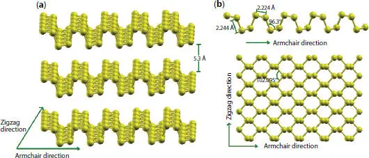
Figure 1.1 Optimized crystallographic structure of (a) 3D BP and (b) 2D BP.
Measurements made by means of preliminary X-ray investigations indicate lattice constants of 3.31 Å and 4.38 Å in ZZ- and AC-axes, respectively, with four atoms forming the unit cell of phosphorene [43, 44]. The experimental result concorde with the theoretical values obtained using ab initio DFT calculations [23, 45].
In phosphorene monolayer, each phosphorus atom is linked to first three nearest neighbor atoms to constitute an sp 3hybridization in a covalent bound [10]. The non-planar geometry leads to two types of bonding, namely, the in-plane bond length d 1is about 2.224 Å , and the out-of-plane bond length d 2that is 2.244 Å, as illustrated in Figure 1.1b. The binding angles y and x are 96.3° and 102.095°, respectively. The height difference between the two half-layers is dz = 2.10 Å .
1.2.2 Physical Properties
1.2.2.1 Anisotropic Eectronic Behavior
Pristine phosphorene is a p-type semiconductor with a direct band gap [13, 46–48]. By using polarization-resolved photoluminescence excitation spectroscopy at room temperature, the quasi-particle band gap of phosphorene is measured to be 2.2 eV [49]. The same value is observed with the typical tunneling spectra of U-shaped electronic spectra [48].
Pure phosphorene has no spin polarization, which is confirmed by symmetrical density of spin-up and -down states displayed in Figure 1.2b. Meanwhile, Figure 1.2ashows that the band dispersion is highly anisotropic around the electronic gap. Indeed, one can observe a much greater dispersion along the Γ-X direction for CBM and VBM with respect to the vertical bands in Γ-Y region. The partial density of states (p-DOS) plots clearly show that p x orbital contribute mainly in the states of the unfilled C-band, while the p z orbital of phosphorus dominates the valence band states [50]. The number of layers mainly affects the gap energy [24]. For instance, it takes the values of 1.51, 0.59, and 0.3 eV for the monolayer, the five layers, and the bulk black phosphorus [51]. Furthermore, the gap energy decreases with increasing the magnitude of external electrical field, which breaks the out-of-plane symmetry. Under biaxial strain and the two possible uniaxial strains, the deformed phosphorene shows a transition from the semiconducting to metallic phase [23].
Читать дальшеИнтервал:
Закладка:
Обсуждение, отзывы о книге «2D Monoelements» и просто собственные мнения читателей. Оставьте ваши комментарии, напишите, что Вы думаете о произведении, его смысле или главных героях. Укажите что конкретно понравилось, а что нет, и почему Вы так считаете.