Liliana Andrade - Multi-Processor System-on-Chip 1
Здесь есть возможность читать онлайн «Liliana Andrade - Multi-Processor System-on-Chip 1» — ознакомительный отрывок электронной книги совершенно бесплатно, а после прочтения отрывка купить полную версию. В некоторых случаях можно слушать аудио, скачать через торрент в формате fb2 и присутствует краткое содержание. Жанр: unrecognised, на английском языке. Описание произведения, (предисловие) а так же отзывы посетителей доступны на портале библиотеки ЛибКат.
- Название:Multi-Processor System-on-Chip 1
- Автор:
- Жанр:
- Год:неизвестен
- ISBN:нет данных
- Рейтинг книги:4 / 5. Голосов: 1
-
Избранное:Добавить в избранное
- Отзывы:
-
Ваша оценка:
Multi-Processor System-on-Chip 1: краткое содержание, описание и аннотация
Предлагаем к чтению аннотацию, описание, краткое содержание или предисловие (зависит от того, что написал сам автор книги «Multi-Processor System-on-Chip 1»). Если вы не нашли необходимую информацию о книге — напишите в комментариях, мы постараемся отыскать её.
Multi-Processor System-on-Chip 1 — читать онлайн ознакомительный отрывок
Ниже представлен текст книги, разбитый по страницам. Система сохранения места последней прочитанной страницы, позволяет с удобством читать онлайн бесплатно книгу «Multi-Processor System-on-Chip 1», без необходимости каждый раз заново искать на чём Вы остановились. Поставьте закладку, и сможете в любой момент перейти на страницу, на которой закончили чтение.
Интервал:
Закладка:
2.3.1. Global architecture
The MPPA3 processor architecture (Figure 2.7) applies the defining principles of many-core architectures: processing elements (SCs on a GPGPU) are regrouped with a multi-banked local memory and a slice of the memory hierarchy into compute units (SMs on a GPGPU), which share a global interconnect and access to external memory. The distinguishing features of the MPPA many-core architecture compared to the GPGPU architecture are the integration of fully software-programmable cores for the processing elements, and the provision of an RDMA engine in each compute unit.
The structuring of the MPPA3 architecture into a collection of compute units, each comparable to an embedded multi-core processor, is the main feature that enables the consolidation of application partitions operating at different levels of functional safety and cyber-security, on a single processor. This feature requires provision of global interconnects with support for partition isolation. From experience with previous MPPA processors, it became apparent that chip global interconnects implemented as “network-on-chip” (NoC) may be specialized for two different purposes: generalization of busses and integration of macro-networks (Table 2.2).
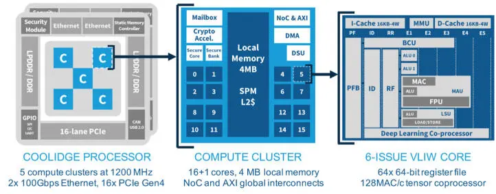
Figure 2.7. Overview of the MPPA3 processor
Table 2.2. Types of network-on-chip interconnects
| Generalized busses | Integrated macro-network |
| Connectionless | Connection-oriented |
| Address-based transactions | Stream-based transactions |
| Flit-level flow control | [End-to-end flow control] |
| Implicit packet routing | Explicit packet routing |
| Inside coherent address space | Across address spaces (RDMA) |
| Coherency protocol messages | Message multicasting |
| Reliable communication | [Packet loss or reordering] |
| QoS by priority and aging | QoS by traffic shaping |
| Coordination with the DDR controller | Termination of macro-networks |
Accordingly, the MPPA3 processor is fitted with two global interconnects, respectively identified as “RDMA NoC” and “AXI Fabric” (Figure 2.8). The RDMA NoC is a wormhole switching network-on-chip, designed to terminate two 100 Gbps Ethernet controllers, and to carry the remote DMA operations found in supercomputer interconnects or communication libraries such as SHMEM (Hascoët et al . 2017). The AXI Fabric is a crossbar of busses with round-robin arbiters, which connects the compute clusters, the external DDR memory controllers, the PCIe controllers and other I/O controllers. The main I/O interfaces of the MPPA3 processor are a PCI Express subsystem with 16 Gen1/Gen2/Gen3/Gen4 lanes for a peak throughput of 32 GB/s full-duplex, and an Ethernet subsystem composed of two controllers of four lanes each, for a total peak throughput of 200 Gbps full-duplex. Other high-speed I/O are supported by four CAN 2.0A/2.0B/FD controllers, and by two USB 2.0 OTG ULPI controllers.
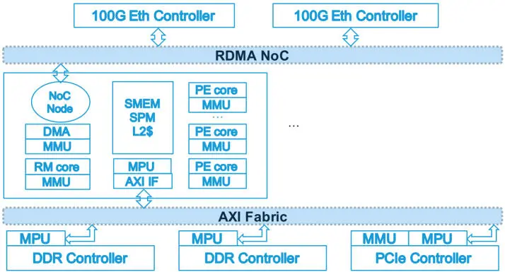
Figure 2.8. Global interconnects of the MPPA3 processor
Based on this global architecture, the consolidation of functions operating at different levels of functional safety and cyber-security is supported by two mechanisms:
– Memory protection units (MPUs) are provided on the AXI Fabric targets to filter transactions based on their machine addresses. Similarly, selected NoC router links can be disabled. This second mechanism has its parameters set at boot time, and then cannot be overridden without resetting the processor. Its purpose is to partition the processor and its peripherals into physically isolated domains, as in the unmanned aerial vehicle applications discussed in section 2.2.
– Cores and other bus initiators have their address translated from virtual to machine addresses by memory management units (MMUs). These MMUs actually implement a double translation: from virtual to physical, as directed by the operating system or the execution environment; from physical to machine, under the control of a partition monitor operating at the hypervisor privilege level. This first mechanism supports the requirements of isolating safety-critical application partitions in multi-core processors (CAST 2016).
2.3.2. Compute cluster
The compute unit of the MPPA3 processor, called the compute cluster, is structured around a local interconnect (Figure 2.9); it comprises a secure zone and a non-secure zone. The secure zone contains a security and safety management core (RM), a 256 KB dedicated memory bank and a cryptographic accelerator. The RM core of each compute cluster is also connected to the processor CSM and the internal boot ROM
through a private bus. The purpose of the secure zone is to host a trusted execution environment (TEE), and a run-time system that performs on-demand code decryption for the applications that require it (Table 2.1). The non-secure zone contains 16 application cores (PE) that share a 16-banked local memory (SMEM), a DMA engine, a debug support unit (DSU), a cryptographic accelerator and cluster-local peripheral control registers. The SMEM can be configured to split its 4 MB capacity between scratch-pad memory (SPM) and level-2 cache (L2$). The non-secure zone of the MPPA3 compute cluster supports two types of execution environments:
– A symmetric multi-processing (SMP) environment, exposed through the standard POSIX multi-threading (supporting the OpenMP run-time of C/C++ compilers) and file system APIs. In this environment targeting high-performance computing under soft real-time constraints, all the core L1 data caches are kept coherent, and the local memory is interleaved across the banks at 64-byte granularity for the SPM and at 256-byte granularity for the L2$.
– An asymmetric multi-processing (AMP) environment, seen as a collection of 16 cores where each executes under an RTOS and is associated through linker maps with one particular bank (256KB) of the local memory. In this environment targeting high-integrity computing under hard real-time constraints, L1 cache coherence is disabled, and the local memory is configured as scratch-pad memory only.
By default, the L2 caches of the compute clusters are not kept coherent, although this can be enabled by running cache controller firmware in the RM cores and maintaining a distributed directory in the cluster SPMs. The third level of the memory hierarchy is composed of the external DDR memory (2x DDR4/LPDDR4 64-bit channels), and of the SPM of other compute clusters. The DDR memory channels can be interleaved or separated in machine address space, in the latter case operating independently. The standard C11 atomic operations are available in all memory spaces.
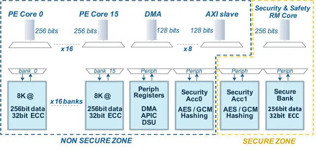
Figure 2.9. Local interconnects of the MPPA3 processor
2.3.3. VLIW core
The MPPA cores implement a 64-bit VLIW architecture, which is an effective way to design instruction-level parallel cores targeting numerical, signal and image processing (Fisher et al . 2005). The VLIW core has six issue lanes (Figure 2.10) that, respectively, feed a branch and control unit (BCU), two 64-bit ALUs, a 128-bit FPU, a 256-bit load–store unit (LSU) and a deep learning coprocessor. Each VLIW core has private L1 instruction and data caches, both 16 KB and four-way set associated with LRU replacement policy. All load instructions also have an L1 cache-bypass variant for direct access to the cluster SPM or L2$. These instructions improve the performance of codes with non-temporal memory access patterns, and also increase the accuracy of static analysis for computing worst-case execution time (WCET) bounds. The implementation of this VLIW core and its caches ensure that the resulting processing element is timing-compositional, a critical property with regard to computing accurate bounds on worst-case response times (WCRT) (Kästner et al . 2013).
Читать дальшеИнтервал:
Закладка:
Похожие книги на «Multi-Processor System-on-Chip 1»
Представляем Вашему вниманию похожие книги на «Multi-Processor System-on-Chip 1» списком для выбора. Мы отобрали схожую по названию и смыслу литературу в надежде предоставить читателям больше вариантов отыскать новые, интересные, ещё непрочитанные произведения.


Обсуждение, отзывы о книге «Multi-Processor System-on-Chip 1» и просто собственные мнения читателей. Оставьте ваши комментарии, напишите, что Вы думаете о произведении, его смысле или главных героях. Укажите что конкретно понравилось, а что нет, и почему Вы так считаете.