Electrical and Electronic Devices, Circuits, and Materials
Здесь есть возможность читать онлайн «Electrical and Electronic Devices, Circuits, and Materials» — ознакомительный отрывок электронной книги совершенно бесплатно, а после прочтения отрывка купить полную версию. В некоторых случаях можно слушать аудио, скачать через торрент в формате fb2 и присутствует краткое содержание. Жанр: unrecognised, на английском языке. Описание произведения, (предисловие) а так же отзывы посетителей доступны на портале библиотеки ЛибКат.
- Название:Electrical and Electronic Devices, Circuits, and Materials
- Автор:
- Жанр:
- Год:неизвестен
- ISBN:нет данных
- Рейтинг книги:3 / 5. Голосов: 1
-
Избранное:Добавить в избранное
- Отзывы:
-
Ваша оценка:
Electrical and Electronic Devices, Circuits, and Materials: краткое содержание, описание и аннотация
Предлагаем к чтению аннотацию, описание, краткое содержание или предисловие (зависит от того, что написал сам автор книги «Electrical and Electronic Devices, Circuits, and Materials»). Если вы не нашли необходимую информацию о книге — напишите в комментариях, мы постараемся отыскать её.
This outstanding new volume presents the basic concepts and fundamentals behind devices, circuits, and systems. It is a valuable reference for the veteran engineer and a learning tool for the student, the practicing engineer, or an engineer from another field crossing over into electrical engineering. It is a must-have for any library.
Electrical and Electronic Devices, Circuits, and Materials — читать онлайн ознакомительный отрывок
Ниже представлен текст книги, разбитый по страницам. Система сохранения места последней прочитанной страницы, позволяет с удобством читать онлайн бесплатно книгу «Electrical and Electronic Devices, Circuits, and Materials», без необходимости каждый раз заново искать на чём Вы остановились. Поставьте закладку, и сможете в любой момент перейти на страницу, на которой закончили чтение.
Интервал:
Закладка:
(2.4) 
Figure 2.11shows the variation of exiting capacitances of hetero and homo DG -TFET with applied gate voltage ( VGS ). The gate-gate capacitance is mainly composed of two capacitances between, gate-drain ( Cgd ), gate-source ( Cgs ) and gate-gate ( Cgg ). The gatesource capacitance (C gs) is lower because of the presence of the tunnel effect, the gate-drain capacitance (C gd) is a dominant capacitance due to the accumulation of the electrons of the source-channel and collected by the drain region.
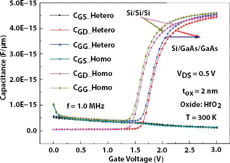
Figure 2.11 The varibility of C-V characteristics with applied gate drive voltage (V GS) and compersion of homo and hetero structure DG -TFET.
As an important circuit design parameter, the cut-off frequency ( f T) is used to evaluate the frequency characteristics of electronic devices. It can be obtained by the ratio of gm to Cgg , with following relation, Equation 2.5
(2.5) 
Figure 2.11shows a variability study of available capacitance on DG -TFET with applied VGS . From Figure 2.11, it has been observed that, as the applied gate voltage increases ( VGS ), the cut-off frequency ( f T) increases to reach its maximum, then with increasing Cgg , it goes down, when the gate voltage ( VGS ) reaches 2.0 V the cut-off frequency ( f T) becomes constant. This is because the on-state current (I ON) and its derivative, g mvalue increase with the electronic B2B tunneling. The cut-off frequency ( f T) of hetero DG-TFET is much larger than that of homo (i.e. f T - hetero~ 0.65 GHz > f T - homo~ 0.55GHz); this is due to smaller Cgg of hetero DG - TFET and the larger of the gm value than homo DG -TFET. This observation is verified by obtained results, shown in Figure (2.8 & 2.11). From these figures, it has been observed that the obtained results predicts decreased gate capacitance with decreased applied gate voltage ( VGS ), as depicted in Figure 2.11, which gives the variation of the gate capacitance with VGS . It should be noted that the capacitances of TFET is bias-dependent. That is to say, the decrement rate of the gate capacitance with frequency is bias-dependent.
The gain bandwidth ( GBW ) product is an important design parameter in the analysis of RF characteristics, which can be calculated by the Equation 2.6. All the results of the simulation are summarized in Table 2.5. As shown in Figure 2.12and Figure 2.13, there is a variation of gm and GWB versus applied gate voltage (V GS) i.e., ( gm , GWB vs. V GS) and compression for homo and hetero DG -TFET. The variation of g m, GWB with V GSis similar to variation of g m, f Twith V GSfrom Figure 2.12and Figure 2.13; clearly, it has been observed that hetero and homo structures transconductance, gain bandwidth product (g m, GWB) increase rapidly as external applied gate voltage V GSincreases.
(2.6) 
The maximum, GWB hetero~ 0.66 GHz and GWB homo~ 0.49 GHz. Another design parameter, the transconductance efficiency (g m/I DS)of for DG - TFET, shown in Figure 2.14, has been calculated. The factor g m/I DSplays a primary role in the behavior of the device; it shows the rate of amplification of the transistor. The g m/I DSof TFETs is dependent on several factors such as drain current (I DS) and SS, barrier tunnel with (λ) i.e., applied gate voltage (V GS). Figure 2.14shows the g m/I DSdependence of applied gate voltage (V GS). As shown in Figure 2.14, g m/I DSincreases until it reaches a maximum value (around the threshold voltage). Figure 2.14shows (g m/I DS) hetero> (g m/I DS) homo. The maximum value of g m/I DS~ 285.84 V -1for hetero structure while ~ 241.01 V -1for homo respectively.
Table 2.5Lists of the computed RF parameters of the hetero and homo DG-TFET.
| High-k gate dielectric HfO2 (≈ 25) | VDS = 0.5 V | |
| Cut-off frequency (fT) | GBW (GHz) | |
| Hetero structure | ~ 0.65 GHz | 0.66 GHz |
| Homo structure | ~ 0.55GHz | 0.49 GHz |
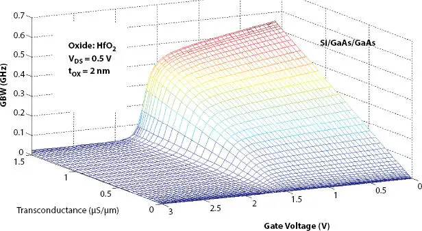
Figure 2.12 3D - transconductance (g m), GBW and applied gate drive voltage (V GS) of hetero DG -TFET.
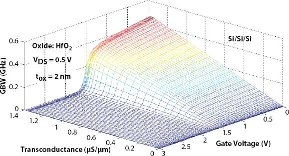
Figure 2.13 3D - transconductance (g m), GBW and applied gate drive voltage (V GS) of homo DG -TFET.
Another important performance parameter for RF analysis is transit time (ι d) estimated by Equation 2.7. The Equation 2.7indicates that the delay time is inversely proportional to the cut-off frequency ( f T) i.e., the cut-off frequency increases as the transition time decreases. It is the time taken by the charge carriers (electrons) to cross the channel. Figure 2.15shows the dependency of applied gate drive voltage (V GS) vs. delay time (ι d) and compression of delay time between homo and hetero structure DG - TFET.
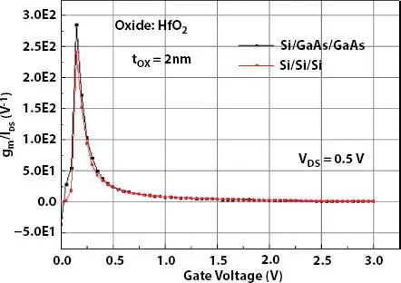
Figure 2.14 Transconductance efficiency, gm/IDS with applied gate voltage ( VGS ) and comparison between double gate hetero and homo structure DG -TFET.
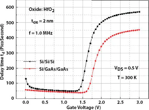
Figure 2.15 Sensitivity of delay time with applied gate voltage (V GS) and comparison between double gate hetero and homo structure DG -TFET.
From Figure 2.15, it has been evident that ι d- hetero< ι d- homoand shows, dealy time with applied gate voltage (V GS) is less sensitive than homo DG-TFT. This is a strong recommendation for low power applications.
(2.7) 
Figure 2.16shows the sensitivity of power delay product (PDP) with applied V GSand a comparison between double gate hetero and homo structure DG -TFET. In term of digital circuit design, power delay product is an important design parameter, correlated with the energy efficiency. From Figure 2.16, it has been observed that PDP is strongly affected with the variation of gate drive voltage (V GS). Lowering the supply voltage (V DS= 0.5V), lowers the PDP in hetero structure DG -TFET.
Читать дальшеИнтервал:
Закладка:
Похожие книги на «Electrical and Electronic Devices, Circuits, and Materials»
Представляем Вашему вниманию похожие книги на «Electrical and Electronic Devices, Circuits, and Materials» списком для выбора. Мы отобрали схожую по названию и смыслу литературу в надежде предоставить читателям больше вариантов отыскать новые, интересные, ещё непрочитанные произведения.


Обсуждение, отзывы о книге «Electrical and Electronic Devices, Circuits, and Materials» и просто собственные мнения читателей. Оставьте ваши комментарии, напишите, что Вы думаете о произведении, его смысле или главных героях. Укажите что конкретно понравилось, а что нет, и почему Вы так считаете.