Electrical and Electronic Devices, Circuits, and Materials
Здесь есть возможность читать онлайн «Electrical and Electronic Devices, Circuits, and Materials» — ознакомительный отрывок электронной книги совершенно бесплатно, а после прочтения отрывка купить полную версию. В некоторых случаях можно слушать аудио, скачать через торрент в формате fb2 и присутствует краткое содержание. Жанр: unrecognised, на английском языке. Описание произведения, (предисловие) а так же отзывы посетителей доступны на портале библиотеки ЛибКат.
- Название:Electrical and Electronic Devices, Circuits, and Materials
- Автор:
- Жанр:
- Год:неизвестен
- ISBN:нет данных
- Рейтинг книги:3 / 5. Голосов: 1
-
Избранное:Добавить в избранное
- Отзывы:
-
Ваша оценка:
Electrical and Electronic Devices, Circuits, and Materials: краткое содержание, описание и аннотация
Предлагаем к чтению аннотацию, описание, краткое содержание или предисловие (зависит от того, что написал сам автор книги «Electrical and Electronic Devices, Circuits, and Materials»). Если вы не нашли необходимую информацию о книге — напишите в комментариях, мы постараемся отыскать её.
This outstanding new volume presents the basic concepts and fundamentals behind devices, circuits, and systems. It is a valuable reference for the veteran engineer and a learning tool for the student, the practicing engineer, or an engineer from another field crossing over into electrical engineering. It is a must-have for any library.
Electrical and Electronic Devices, Circuits, and Materials — читать онлайн ознакомительный отрывок
Ниже представлен текст книги, разбитый по страницам. Система сохранения места последней прочитанной страницы, позволяет с удобством читать онлайн бесплатно книгу «Electrical and Electronic Devices, Circuits, and Materials», без необходимости каждый раз заново искать на чём Вы остановились. Поставьте закладку, и сможете в любой момент перейти на страницу, на которой закончили чтение.
Интервал:
Закладка:
Keywords:TFET, MOSFET, BTBT, SCEs, Kane’s model, high - k, subthreshold (SS), Ultra low power
2.1 Introduction
Since the last few decades, the electronics industry has enjoyed conventional MOSFET due to aggressive scaling property. This “aggressive scaling” progress concept with conventional MOSFET , has also produced numerous challenges briefly known as short channel effects ( SCEs ) [1–5]. In addition, the current mechanism in MOSFETs is controlled by a drift-diffusion, a conventional charge transport phenomenon popularly known as thermionic emission of charge carriers in ultra-scaled MOSFETs [3–5]. The drift-diffusion of high-energy charge carriers in ultra-scaled MOSFETs follow the Fermi–Dirac distribution and hence have an energy slope of kT (where k is the Boltzmann constant, T is the absolute temperature). This is a technical reason that conventional MOSFET causes subthreshold slope limitation, SS > 60 mV/decade at room temperature. This technical barrier in the progress path of electronic industry with conventional MOSFETs causes a bottleneck issue for semiconductor players. In addition, a quantum transport mechanism known as tunneling between band-to-band ( B2B ) in the ultra-scaled field effect devices, does not suffer such limitations imposed by the Boltzmann [3–8]. This transport mechanism allow further scaling of FET devices with scaled power supply ( VDD ) [9–12], which makes tunneling device the most promising alternative for the conventional MOSFETs for low-power circuit and system applications.
Unlike conventional MOSFETs , TFETs are basically an asymmetrical source/drain highly doped FET device. The basic structure of TFET device is derived and developed by p-i-n diode [10, 11], containing two heavily doped degenerated semiconductor “p” and “n” regions and lightly doped intrinsic “i” region, respectively. It is commonly operated in reverse biased condition. The current generation in tunneling devices is enabled by the band-to-band ( B2B ) tunneling mechanism between the source to drain region via channel [13–17].
However, the lower switching current due to limited tunneling charge carriers in tunnel FET devices than conventional MOSFETs has become problematic for solving limitations of conventional MOSETs [3–8]. To obtain the improved electrical characteristics in terms of current efficiency ( ION ), leakage current ( IOFF ), subthreshold slope ( SS ), transconductance ( gm ), switching response time etc., several ideas have been proposed by scientists and semiconductor players. Gate dielectric and bandgap engineering were the most popular key ideas [18–25]. As per requirements and state-of-the-art modern ultra-low-power electronics, this chapter is dedicated to double gate tunnel FET ( DG -TFET ), circuit and system design. In this chapter, we explore the idea of high-k dielectric engineering as well as band engineering concept with DG -TFET . A detailed investigation has been done for the requirements for ultra-low-power circuit and system design based on DG -TFET .
2.2 Fundamental of Device Physics
2.2.1 Basic Working Principles of TFET
Tunnel FET is a type of field effect device in which current transport phenomena occur due to quantum tunneling between source and channel. The band-to-band ( B2B ) tunneling current ( IDS ) of TFET devices is governed by following Equation 2.1[15–26]. The tunneling probability T(E) is given by WKB (Wentzel-Kramers- Brillouin) approximation.
(2.1) 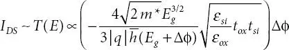
Here in Equation 2.1, m * is the effective mass of charge particle, Eg is band gap, ΔΦ is the energy range for B2B Tunneling window over which tunneling can take place. And collectively tox, tsi, εox, εsi known as device design parameters called the oxide and silicon films thickness and dielectric constants, respectively. The remaining constant such as “ ћ ” is called reduced Planck’s constant, “| q| ” known as electronic charge. The tunneling window (Δ Φ ) in the tunneling probability can be also expressed: 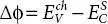 . As shown, Equation 2.1has a unique property, which provides full facilities for a process engineer to optimize device characteristics, which is useful for circuit design purpose for optimization of an advanced low-power circuit and system such as IoTs .
2.2.2 Kane’s Model
The band-to-band ( B2B ) tunneling current (I BTBT) in tunneling FET can be obtained from the following Equation 2.2[27–30].
(2.2) 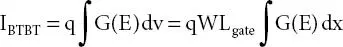
As shown in Equation 2.2, W and Lgate are width and gate length TFET devices, respectively. The G (E) is generation rate of charge in tunneling FET. It is basically the number of the carriers per unit volume per unit time. The generation rate of charge carrier per unit volume per unit time can be calculated by the well-known Kane’s Model.
(2.3) 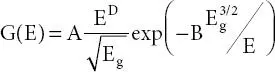
As shown in Equation 2.3A, B and D are material dependent parameters of Kane’s model. E is the electric field in the device.
2.3 Analysis Approach and Device Parameters
Practically, the estimation of device characteristics and performance of TFET is still time consuming and costly due to lack of rapid advancement in technology. The conventional procedure commonly used in electronic industry known as “Modeling and Simulation” is adopted for DG - TFET device. This is practically a more adequate procedure and a relatively inexpensive way to design electronic circuit and system.
The results shown in this chapter are taken from Silvaco ATLAS TMsimulation. For accurate estimation of device performance, the non-local BTBT (BBT.NONLOCAL) model has been used to estimate the tunneling current in DG - TFET . In addition, SRH (Shokely-Read-Hall) recombination, auger recombination, trap-assisted tunneling (TAT) and band gap narrowing ( BGN ) model has been incorporated.
Figure 2.1shows the schematic view of double gate TFET ( DG - TFET ). As shown in Figure 2.1in hetero DG - TFET , source and channel region contains heavily doped semiconductors with two different band gap semiconductors, Si (Eg~1.12eV) and GaAs (Eg~1.52eV). As per state-of-art of bandgap engineering, at the interface region of Si/GaAs , the effective bandgap (E g effective) is slightly smaller than homo Si or GaAs . According to Equation 2.1, this reduced Eg effectiveincreases the tunneling probability, results larger tunneling current in hetero TFET than homo TFET. The representative schematic diagram of hetero and homo DG - TFET is shown in Figure 2.1(a)and Figure 2.1(b)containing Si/GaAs/GaAs and Si/Si/Si semiconductor materials in source, channel and the drain region, respectively. For the improvement of electrostatic behavior DG - TFET , suggested by K . Boucart et al. [26], here HfO2 dielectric has been used as a key gate material. As shown in Figure 2.1the DG -TFET device, which is calibrated with simulated structure with a channel length (L ch) of 50 nm, ultra-thin body (t si) of 10 nm.
Читать дальшеИнтервал:
Закладка:
Похожие книги на «Electrical and Electronic Devices, Circuits, and Materials»
Представляем Вашему вниманию похожие книги на «Electrical and Electronic Devices, Circuits, and Materials» списком для выбора. Мы отобрали схожую по названию и смыслу литературу в надежде предоставить читателям больше вариантов отыскать новые, интересные, ещё непрочитанные произведения.


Обсуждение, отзывы о книге «Electrical and Electronic Devices, Circuits, and Materials» и просто собственные мнения читателей. Оставьте ваши комментарии, напишите, что Вы думаете о произведении, его смысле или главных героях. Укажите что конкретно понравилось, а что нет, и почему Вы так считаете.