Electrical and Electronic Devices, Circuits, and Materials
Здесь есть возможность читать онлайн «Electrical and Electronic Devices, Circuits, and Materials» — ознакомительный отрывок электронной книги совершенно бесплатно, а после прочтения отрывка купить полную версию. В некоторых случаях можно слушать аудио, скачать через торрент в формате fb2 и присутствует краткое содержание. Жанр: unrecognised, на английском языке. Описание произведения, (предисловие) а так же отзывы посетителей доступны на портале библиотеки ЛибКат.
- Название:Electrical and Electronic Devices, Circuits, and Materials
- Автор:
- Жанр:
- Год:неизвестен
- ISBN:нет данных
- Рейтинг книги:3 / 5. Голосов: 1
-
Избранное:Добавить в избранное
- Отзывы:
-
Ваша оценка:
Electrical and Electronic Devices, Circuits, and Materials: краткое содержание, описание и аннотация
Предлагаем к чтению аннотацию, описание, краткое содержание или предисловие (зависит от того, что написал сам автор книги «Electrical and Electronic Devices, Circuits, and Materials»). Если вы не нашли необходимую информацию о книге — напишите в комментариях, мы постараемся отыскать её.
This outstanding new volume presents the basic concepts and fundamentals behind devices, circuits, and systems. It is a valuable reference for the veteran engineer and a learning tool for the student, the practicing engineer, or an engineer from another field crossing over into electrical engineering. It is a must-have for any library.
Electrical and Electronic Devices, Circuits, and Materials — читать онлайн ознакомительный отрывок
Ниже представлен текст книги, разбитый по страницам. Система сохранения места последней прочитанной страницы, позволяет с удобством читать онлайн бесплатно книгу «Electrical and Electronic Devices, Circuits, and Materials», без необходимости каждый раз заново искать на чём Вы остановились. Поставьте закладку, и сможете в любой момент перейти на страницу, на которой закончили чтение.
Интервал:
Закладка:
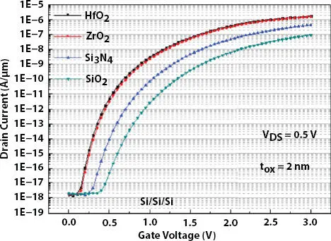
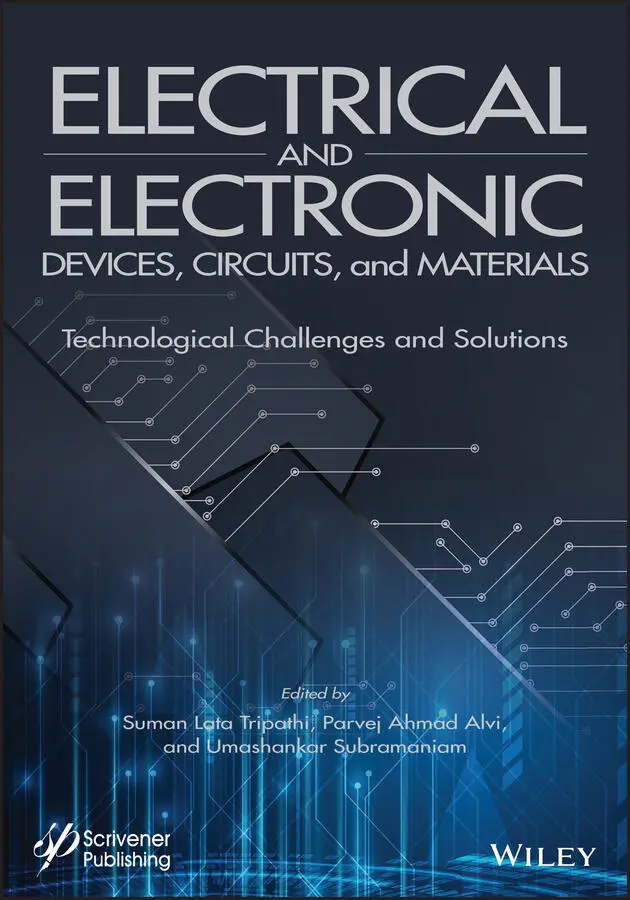
Figure 2.4 Transfer characteristic of homo structure double gate TFET.
Figure 2.5 Transfer characteristic of hetero structure double gate TFET.
Table 2.3Lists of computed design parameters of the homo structure DG -TFET with various gate dielectric materials.
| Design parameters | Gate dielectric material (Homo structure Si/Si/Si) | |||
| HfO2 (k ≈ 25) | ZrO2 (k ≈ 24) | Si3N4 (k ≈ 12) | SiO2 (k ≈ 3.9) | |
| Vth(V) | 0.55 | 0.55 | 0.80 | 0.85 |
| SS(mV/decade) | 39.68 | 39.71 | 42.73 | 45.00 |
| ION(A/μm) | 4.0 × 10 -6 | 3.90 × 10 -6 | 5.00 × 10 -7 | 1.00 × 10 -7 |
| IOFF(A/μm) | 1.00 × 10 -18 | 1.00 × 10 -18 | 1.00 × 10 -18 | 1.00 × 10 -18 |
| ION/IOFF | 4.00 × 10 12 | 3.90 × 10 13 | 5.0 × 10 11 | 1.00 × 10 11 |
Table 2.4Lists of computed design parameters of the hetero structure DG -TFET with various gate dielectric materials.
| Design parameters | Gate dielectric materials (Hetero structure Si/GaAs/GaAs) | |||
| HfO2 (k ≈ 25) | ZrO2 (k ≈ 24) | Si3N4 (k ≈ 12) | SiO2 (k ≈ 3.9) | |
| Vth (V) | 0.5 | 0.5 | 0.7 | 0.75 |
| SS(mV/decade) | 34.25 | 34.27 | 40.65 | 44.25 |
| ION(A/μm) | 4.00 × 10 -6 | 3.90 × 10 -6 | 2.00 × 10 -7 | 2.00 × 10 -8 |
| IOFF(A/μm) | 1.00 × 10 -20 | 1.00 × 10 -19 | 1.00 × 10 -19 | 1.00 × 10 -19 |
| ION/IOFF | 4.00 × 10 14 | 3.90 × 10 14 | 2.0 × 10 12 | 2.00 × 10 11 |
Ideally in off-state, there is no current flow in TFET , due to large tunneling width ( λ ). But in practical case, few charge particles pass the λ, in off-state condition, resulting in smaller IOFF current. But practically the magnitude of the off current in case of TFET is smaller than MOSFETs. On the other hand, when applied VGS sufficiently large, tunneling barrier λ, between source and channel reduce significantly and sufficient number of charge particles to pass from source to drain via channel, resulting in ION current. Interestingly, when applied VGS is negatively high, the tunneling barrier width between the channel and drain narrows, which induces tunneling current [17–22]. The particular state of TFET device is known as ambipolar state and the amount of current following in this state is known as ambipolar ( Iamb ), as shown in Figure 2.6. Figure 2.6is dedicated for study of ambimiparity behaviour of DG -TFET , an unwanted conduction known as malfunction. Figure 2.6shows the comparision of ambipolar property of homo and hetero structure DG - TFET . The result shows that, DG -TFET with adopted technology shows suppression of the ambipolar current ( Iamb ) without deteriorating analog, and transient performance. From Figure 2.6, it has been observed, with the help of 2-D. TCAD simulation that, the ambipolar current ( Iamb ) is suppressed by 10 8order of magnitude in proposed Si/GaAs/GaAs hetero DG - TFET as compared to Si/Si/Si homo DG -TFET up to the applied gate voltage of V GS= − 3.0V the step of gate voltage was taken equal to 0.5V.
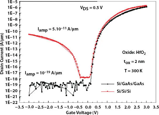
Figure 2.6 Comparision of ambipolar current vs. applied gate drive voltage (V GS) for homo and hetero structure double gate tunnel FET.
Figure 2.7shows the impact of drain voltage ( VDS ) on DG -TFET . From Figure 2.7, it is clearly evident that applied drain voltage ( VDS ) has negligible impact on TFET performance. This is strong evidence that TFET is almost free from DIBL (Drain Induced Barrier Lower). This is a strong recommendation for replacement of conventional low-power device, circuit and system with TFETs and TFET-based circuit and system design.
The transconductance ( gm ) represents amplification ability of device and important design parameter of circuit and system design. It is defined as the slope of the transfer characteristic. The gm value can be calculated by mathematical Equation 2.4. Figure 2.8shows the variation of gm versus applied VGS . From Figure 2.8, it has been observed that g mvalue decreases with decrease of applied gate voltage, VGS that is due smaller tunneling current at lower VGS .
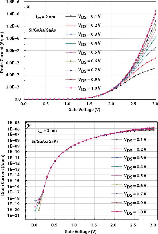
Figure 2.7 Device transfer characteristics for double gate N- TFET hetero structure with a variation of V DSplot (a) linear (b) Semilog.
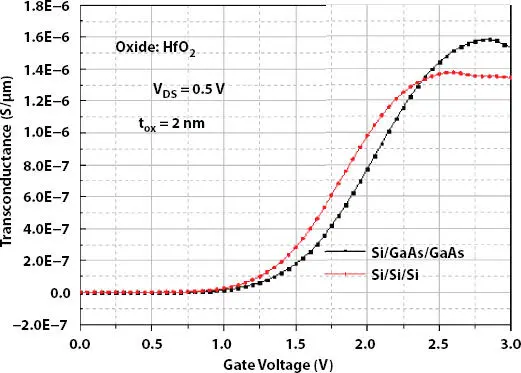
Figure 2.8 Sensitivity of transconductance ( gm ) with applied gate voltage ( VGS ) and comperision between double gate hetero and homo structure DG -TFET.
Figure 2.9shows 3D visualization of transconductance, cut-frequency and applied gate voltage ( gm , f T, VGS ). From Figure 2.9and Figure 2.10, clearly, it has been observed that the hetero and homo structures: transconductance, cut-frequency ( gm , f T) increase rapidly as external applied gate voltage V GSincreases. The maximum gm-hetero value of the hetero DG -TFET ~1.6 μS/μm and f T-hetero~ 0.65 GHz and gm-homo ~1.4 μS/μm f T-homo~ 0.55GHz. The gm-hetero > gm-homo due to smaller effective tunneling barrier width (i.e. λ hetero~ 0.05 µm< λ hetero~0 .056 µm), shown in Figure 2.2and Figure 2.3
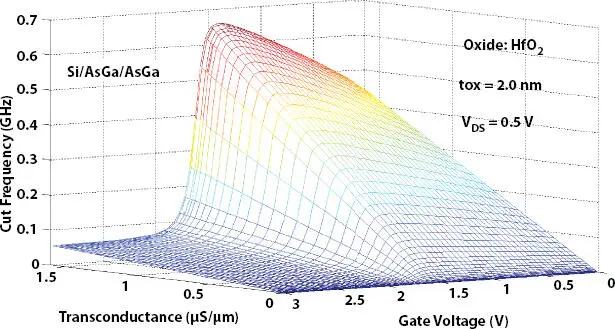
Figure 2.9 3D - transconductance ( gm ), cut-frequency ( fT ) and applied gate drive voltage ( VGS ) of hetero DG -TFET.
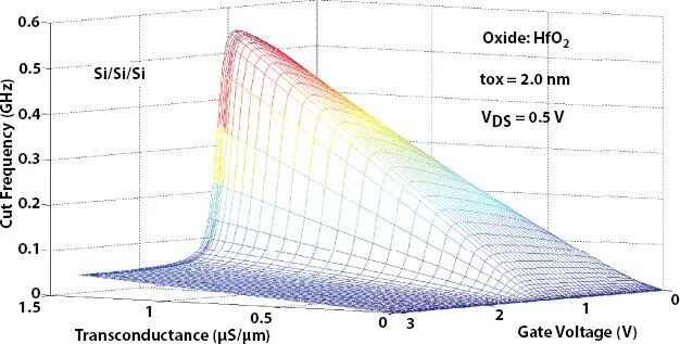
Figure 2.10 3D - transconductance (g m), cut-frequency (f T) and applied gate drive voltage (V GS) of homo DG -TFET.
Читать дальшеИнтервал:
Закладка:
Похожие книги на «Electrical and Electronic Devices, Circuits, and Materials»
Представляем Вашему вниманию похожие книги на «Electrical and Electronic Devices, Circuits, and Materials» списком для выбора. Мы отобрали схожую по названию и смыслу литературу в надежде предоставить читателям больше вариантов отыскать новые, интересные, ещё непрочитанные произведения.


Обсуждение, отзывы о книге «Electrical and Electronic Devices, Circuits, and Materials» и просто собственные мнения читателей. Оставьте ваши комментарии, напишите, что Вы думаете о произведении, его смысле или главных героях. Укажите что конкретно понравилось, а что нет, и почему Вы так считаете.