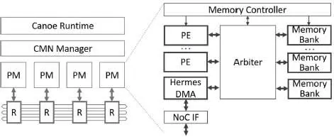
Figure 1.5. Tiled “Kachel” MPSoC with decentralized tightly coupled memories
When it comes to MPSoC architecture in the sense of module arrangement and layout, we have recently published works with both decentralized (e.g. in Figure 1.5, (Fettweis et al . 2019)) and centralized (e.g. in Figure 1.6, (Damjancevic et al . 2019)) memory in mind. Although this chapter follows closely the later work, the programmable vector processor is a common processing element in both, and the lessons learned are universal 13 .
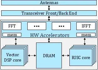
Figure 1.6. Heterogeneous MPSoC with a central shared memory architecture
Without discussing the layouts, as both have their advantages, let us delve into the common thread and analyze the combined effect of workloads and algorithms on HW provisioning requirements and possibly confirm our hypothesis that a heterogeneous MPSoC is required for an efficient future-proof solution.
1.3. GFDM algorithm breakdown
Knowledge of algorithm kernel 14 requirements with respect to workload is key to determining whether or not the vDSP has enough available compute resources to execute the kernel. This section covers the GFDM algorithm and its processing graph extrapolated pseudo-code.
GFDM processing in the literature is divided into three categories:
1 1) frequency-domain processing (Michailow et al. 2014);
2 2) time-domain processing (Farhang et al. 2016; Matthé et al. 2016);
3 3) Radix-2 cascade processing (Nimr et al. 2018).
We assume (2) time-domain processing for implementation on the vDSP, primarily due to its flexibility and low compute complexity per data point on small workloads.
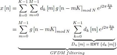
We consider a GFDM resource grid with K subcarriers and M symbols. In total, N = MK complex data symbols are transmitted within a GFDM block, where dk [ m ] represents a data symbol to be transmitted on the kth subcarrier and the mth symbol for k = 0, 1, …, K − 1, m = 0, 1, …, M − 1. The signal corresponding to the kth subcarrier is constructed by K -times up-sampling the data vector dk = [ dk [0], dk [1], …, dk [ M − 1]] T, followed by pulse shape filtering with g [ mK ] and subcarrier modulation  . The resulting GFDM signal x [ n ] for n = lK + i ; l = 0, 1, …, M − 1; i = 0, 1, …, K − 1 is shown in [1.1]
[1-1] 
where l = 0, 1 ,…, M − 1; n = 0, 1 ,…,K − 1 and g [.] mod Nis the impulse response of the K -times over-sampled pulse shaping filter with circular symmetry. Reordering the sums in equation [1.1]leads to a K -point IDFT{ d [ m ]} of the mth data symbol vector d [ m ] = [ d 0 [ m ], d 1 [ m ] ,…, dK− 1 [ m ]] Tand subsequent filtering of IDFT outputs D [ m ] = [ D 0[ m ], D 1[ m ],…, D K–1[ m ]] T. IDFT is a well-researched topic, hence the novelty of interest in our work is the filtering of D [ m ].
1.3.2. Dataflow processing graph and matrix representation
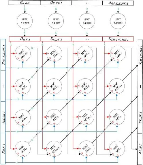
The associated dataflow processing graph is depicted in Figure 1.7, with the notation foo [ bar ] abbreviated as foobar .
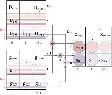
Each multiply-accumulate (MAC) in Figure 1.7 operates on input/output vector length of K elements that results in the total M 2 K scalar MAC operations, 2 M 2 K loads and MK stores. This is the theoretical minimum number of operations. The MAC result is stored in an indexed accumulator register (ACC) and is used in the next MAC of the same index. For readers not familiar with dataflow diagrams, a matrix representation of GFDM filtering is shown in Figure 1.8, and the experience drawn from matrix multiplication implementations can also be used here.

Figure 1.7. GFDM processing dataflow diagram
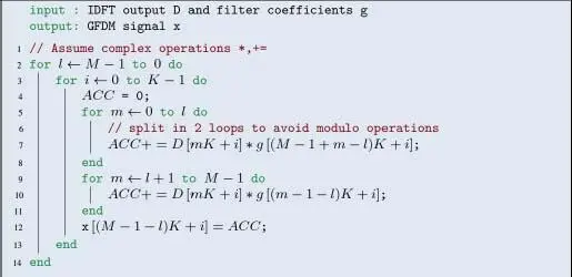
Observing only the equation, a naive programmer could see the modulo load operation on g [.] and get stuck or try to write % for modulo in their C code, hoping that the compiler could deal with it. Fortunately for us, we have drawn the processing graph and can infer the processing required and how to circumvent the modulo operation altogether.

Figure 1.8. Visualization of time-domain GFDM filtering

Figure 1.9. GFDM pseudo-code
GFDM filtering consists of three mutually independent “for” loops (shown in Figure 1.9) 15 . Since the loops are mutually independent, they can be interchanged freely, which effectively changes the processing order to the programmer’s desire. Again, naively, we could think that the order does not matter as long as the “job gets done”, but, as we will see in section 1.5, the loop order has a notable impact on memory and processor utilization when using a vector machine. However, before we discuss different loop orders, we need to investigate fixed-point precision requirements, i.e. bit-lengths required to achieve acceptably low quantization error based on the 4G and 5G standard specification.
1.4. Algorithm precision requirements and considerations
It is often taken for granted that we can take a state-of-the-art (SotA) processor “off-the-shelf” and program the kernel straight without thinking much about data degradation due to quantization noise. Yet even an error as small as a percentile off the true value, compounded over all the succeeding processing steps of the system, may result in faulty data for the user application. Therefore, the standardization body defines the error budget (3GPP 2018b, 2019a), which can be distributed among different processing steps.

Figure 1.10. Precision test bed set up
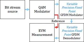
Of interest is determining the necessary number of bits to represent input and output data, as well as the necessary bit-length size of the processor accumulators where intermediate results are stored. Input and output share the same data type (bit-length) since that simplifies memory access, while, for accumulators, we assume a different data type. We denote the bit-lengths for these hypothetical data types as databits and ACCbits for input/output and accumulators, respectively. Assuming a Q0.n: normalized to 1 signed integer notation, where n is the number of fractional bits, we consider the following test bed setup, illustrated in Figure 1.10. A random bit stream is mapped to complex QAM symbols. Next, QAM symbols are mapped to dk in equation [1.1], a copy of dk is kept as reference. QAM symbols are GFDM-modulated using IDFT and filtered as per the algorithm shown in Figure 1.9 and afterwards demodulated. Demodulation is done by repeating the algorithm shown in
Читать дальше


 . The resulting GFDM signal x [ n ] for n = lK + i ; l = 0, 1, …, M − 1; i = 0, 1, …, K − 1 is shown in [1.1]