Liliana Andrade - Multi-Processor System-on-Chip 2
Здесь есть возможность читать онлайн «Liliana Andrade - Multi-Processor System-on-Chip 2» — ознакомительный отрывок электронной книги совершенно бесплатно, а после прочтения отрывка купить полную версию. В некоторых случаях можно слушать аудио, скачать через торрент в формате fb2 и присутствует краткое содержание. Жанр: unrecognised, на английском языке. Описание произведения, (предисловие) а так же отзывы посетителей доступны на портале библиотеки ЛибКат.
- Название:Multi-Processor System-on-Chip 2
- Автор:
- Жанр:
- Год:неизвестен
- ISBN:нет данных
- Рейтинг книги:3 / 5. Голосов: 1
-
Избранное:Добавить в избранное
- Отзывы:
-
Ваша оценка:
Multi-Processor System-on-Chip 2: краткое содержание, описание и аннотация
Предлагаем к чтению аннотацию, описание, краткое содержание или предисловие (зависит от того, что написал сам автор книги «Multi-Processor System-on-Chip 2»). Если вы не нашли необходимую информацию о книге — напишите в комментариях, мы постараемся отыскать её.
Multi-Processor System-on-Chip 2 — читать онлайн ознакомительный отрывок
Ниже представлен текст книги, разбитый по страницам. Система сохранения места последней прочитанной страницы, позволяет с удобством читать онлайн бесплатно книгу «Multi-Processor System-on-Chip 2», без необходимости каждый раз заново искать на чём Вы остановились. Поставьте закладку, и сможете в любой момент перейти на страницу, на которой закончили чтение.
Интервал:
Закладка:
Referring to Figure 1.13, we designed a cycle-accurate simulation model of the vDSP in the ASIP Designer tool suite (Synopsys Inc 2019). The tool comes with a C-compiler and a debugging and profiling environment, which allowed for practical measurements of realistic cycle counts for the GFDM variants implementation. In a reiterative process, we have recursively tuned the prototype, refining the HW architecture instruction set and VLIW configuration, editing functional units of the vDSP, parallel to the development of the black and blue vector codes. We have arrived at an adequate processor and corresponding black and blue optimized code variants. Based on considerations thus far, we define 512 bit SIMD (vector) processing, 16 bit complex data types, 40 bit complex accumulators and 1 GHz clock.
We use theoretical minimum operations as the baseline for a fair, objective and unbiased comparison between the code variants and their utilization of processor resources. We call this metric implementation execution density ρ and define it as a ratio of minimum theoretical operations and measured cycles. The theoretical minimum includes a) only general/standard arithmetic or logical operations (not fused/composite operations that combine several into one, with MAC as the only exception), and b) memory accesses. The theoretical vector operations minimum depends on the implementation variant, i.e. the loop order combination and vectorization.
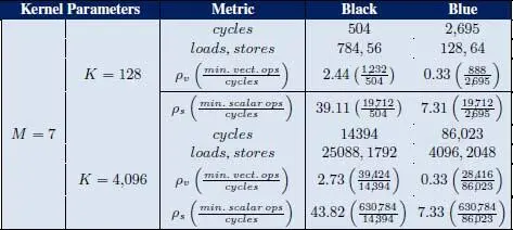
Table 1.4gives us the GFDM kernel profile. The variant-specific minimum operations are taken from Table 1.3for the ρ calculation. From Table 1.4, we can note a) the difference in total memory accesses and cycle counts between the two code variants as a consequence of different loop ordering and loop vectorization; b) even ρv > 1 values are possible when optimizing the low cycle count (black) variant through thoughtful code scheduling on the processor VLIW architecture with multiple instruction issue slots, with 512 bit SIMD capability per slot, and efficient pipelining for the selected loop order and vectorization; and c) ρs shows the ratio between the theoretical best case scalar execution and our kernel and can be interpreted as a speed up against the optimal theoretical scalar processor implementation.
Table 1.4. Kernel profile: cycles, memory accesses, and density
As the last step in our investigation, we show the required frequency budget needed for the corner cases, in Table 1.5. To form the budget requirements, we need to take into account the cycle counts from Table 1.4, as well as number of kernel calls, kernel parameters and deadlines from Table 1.2. Finally, we show the mentioned budget requirement in the context of our vDSP. In particular, how large a portion of the total vDSP frequency budget is needed to meet the specific use case requirements. Higher than 100% usage means that more than 1 vDSP core is needed.
Table 1.5. GFDM: required frequency budget and performance on our vDSP
| Use Case | Metric | Black | Blue |
low-end LTE legacy  |
required budget [ MHz ] | 1.01 | 5.39 |
| our vDSP | processing time [ µs ] | 0.504 | 2.695 |
| vDSP utilization [%] | 0.10 | 0.54 | |
| min. vDSP s to run [#] | 1 | 1 | |
CA high-end FR2  4 × CA, µ = 3,400 MHz 4 × CA, µ = 3,400 MHz |
required budget [ MHz ] | 921.2 | 5,505.5 |
| our vDSP | processing time [ µs ] | 57.58 | 344.09 |
| vDSP utilization [%] | 92.12 | 550.55 | |
| min. vDSP s to run [#] | 1 | 6 | |
MIMO CA high-end FR2  8 ×8, 4 × CA, µ = 3,400 MHz 8 ×8, 4 × CA, µ = 3,400 MHz |
required budget [ MHz ] | 7.37 | 44.04 |
| our vDSP | processing time [ µs ] | 460.6 | 2,752.7 |
| vDSP utilization [%] | 736.95 | 4,404.38 | |
| min. vDSP s to run [#] | 8 | 45 |
The results argue in favor of the discussion from section 1.2: it is practical to run the low-end use cases quite effortlessly in parallel with other kernels and tasks on a vDSP. Surprisingly, even the CA high-end black GFDM can fit on a single vDSP core and make the deadline, albeit at a heavy load. Since there are several vDSPs on the MPSoC, running this modulation flavor is an option to consider, provided, of course, that the memory bandwidth allows using the black flavor. Finally, as expected, it is practical to use HW accelerator engines for the MIMO CA high-end use case instead of many fully loaded vDSP cores.
1.6. Conclusion
This chapter closely followed an SW implementation of the GFDM algorithm on the SotA vDSP and noted considerations taken into account with regard to handset workloads expected in modern and future mobile communications. We give analyses and conclusions on four layers: specification requirements, translating theory to pseudo-code, precision analysis and requirements and implementation space exploration.
First, we indicated trends and analyzed specifications for the most advanced 5G communication standard at the time of writing this chapter and defined workloads based on these specifications. To get closer to HW requirements, we selected an example beyond 5G algorithm GFDM to implement and investigate its HW requirements for those workloads. Second, from the theory behind GFDM, we developed the processing graph and pseudo-code that does not use modulo operations. Third, the precision analysis indicated that HW should be able to handle data types of at least 32 bits (16 bit – real, 16 bit – imag) per data point for operation and that the processor accumulators should have at least [ log 2 M ] guard bits to facilitate computations without degradation. Fourth, we identified the range of kernel parameters as well as the number of calls and deadlines for the low- and high-end 5G workloads, followed by the implementation space exploration, resulting in high-throughput and low-memory access code variants of the same kernel. Finally, the kernel variants and workloads are combined to indicate required HW for corner cases. For the low-end and CA high-end vDSPs are recommended, while for higher than those and towards MIMO CA high-end workloads, more specialized (application-specific) HW accelerators or ASIPs are recommended.
We can see that giving a recommendation or direct HW requirements for SotA specifications is a multi-layered challenge that is difficult to overcome. For the overall system, other kernels can be analyzed in the same manner; however, the overarching theme is the need for variability and flexibility at each step of the analysis. Heterogeneous HW MPSoCs consisting of RISCs, vDSPs, ASIPs and dedicated (application-specific) HW accelerators can provide both flexibility and highly optimized solutions in the power consumption/chip area/chip cost sense, provided that enough care and effort has been invested into the investigation of the above-mentioned layers.
Читать дальшеИнтервал:
Закладка:
Похожие книги на «Multi-Processor System-on-Chip 2»
Представляем Вашему вниманию похожие книги на «Multi-Processor System-on-Chip 2» списком для выбора. Мы отобрали схожую по названию и смыслу литературу в надежде предоставить читателям больше вариантов отыскать новые, интересные, ещё непрочитанные произведения.


Обсуждение, отзывы о книге «Multi-Processor System-on-Chip 2» и просто собственные мнения читателей. Оставьте ваши комментарии, напишите, что Вы думаете о произведении, его смысле или главных героях. Укажите что конкретно понравилось, а что нет, и почему Вы так считаете.