Anand K. Verma - Introduction To Modern Planar Transmission Lines
Здесь есть возможность читать онлайн «Anand K. Verma - Introduction To Modern Planar Transmission Lines» — ознакомительный отрывок электронной книги совершенно бесплатно, а после прочтения отрывка купить полную версию. В некоторых случаях можно слушать аудио, скачать через торрент в формате fb2 и присутствует краткое содержание. Жанр: unrecognised, на английском языке. Описание произведения, (предисловие) а так же отзывы посетителей доступны на портале библиотеки ЛибКат.

- Название:Introduction To Modern Planar Transmission Lines
- Автор:
- Жанр:
- Год:неизвестен
- ISBN:нет данных
- Рейтинг книги:4 / 5. Голосов: 1
-
Избранное:Добавить в избранное
- Отзывы:
-
Ваша оценка:
Introduction To Modern Planar Transmission Lines: краткое содержание, описание и аннотация
Предлагаем к чтению аннотацию, описание, краткое содержание или предисловие (зависит от того, что написал сам автор книги «Introduction To Modern Planar Transmission Lines»). Если вы не нашли необходимую информацию о книге — напишите в комментариях, мы постараемся отыскать её.
rovides a comprehensive discussion of planar transmission lines and their applications, focusing on physical understanding, analytical approach, and circuit models
Planar transmission lines form the core of the modern high-frequency communication, computer, and other related technology. This advanced text gives a complete overview of the technology and acts as a comprehensive tool for radio frequency (RF) engineers that reflects a linear discussion of the subject from fundamentals to more complex arguments.
Introduction to Modern Planar Transmission Lines: Physical, Analytical, and Circuit Models Approach Emphasizes modeling using physical concepts, circuit-models, closed-form expressions, and full derivation of a large number of expressions Explains advanced mathematical treatment, such as the variation method, conformal mapping method, and SDA Connects each section of the text with forward and backward cross-referencing to aid in personalized self-study
is an ideal book for senior undergraduate and graduate students of the subject. It will also appeal to new researchers with the inter-disciplinary background, as well as to engineers and professionals in industries utilizing RF/microwave technologies.
Introduction To Modern Planar Transmission Lines — читать онлайн ознакомительный отрывок
Ниже представлен текст книги, разбитый по страницам. Система сохранения места последней прочитанной страницы, позволяет с удобством читать онлайн бесплатно книгу «Introduction To Modern Planar Transmission Lines», без необходимости каждый раз заново искать на чём Вы остановились. Поставьте закладку, и сможете в любой момент перейти на страницу, на которой закончили чтение.
Интервал:
Закладка:
Figure (5.15a)shows the generation of the radiation cone of the spherical wavefronts by a moving charge, with velocity V c, in a DPS medium. The charged particle velocity V cis greater than the phase velocity V pof the EM‐wave in a DPS medium, i.e. V c> V p( = c/n). The positive refractive index is n, and c is the velocity of EM‐wave in free space. The locations P 0–P 4, on the positive x‐axis, are successive positions of the moving charge at time t 0–t 4. During the time interval T = (t 4− t 0), the spherical wavefront acquires radius P 0N = V pT = (c/n)T, while the charged particle travels a distance P 0P 4= V cT. Figure (5.15a)also shows other spherical wavefronts for the time sequence for t < T. Following the Huygens principle, the inclined tangential wavefront of the secondary radiation is NP 4. The wavevector (k), i.e. P 0N, is normal to the wavefront NP 4. It forms a Cerenkov angle ϕ cat P 0or angle θ cat P 4. It is obtained from the triangle P 0N P 4:
(5.5.41) 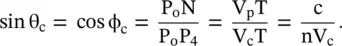
Figure (5.15b)shows the directions of the wavevectors  and Poynting vectors
  of the upper and lower radiation from the charged particle moving in the positive x‐direction. Cerenkov radiation is a linearly polarized EM‐wave with an electric field component parallel to the path of the charged particle, i.e. the x‐axis. Cerenkov radiation is directive in the forward direction within the cone angle 2ϕ c. Similarly, a leaky‐wave antenna is highly directive. The beam becomes narrower for the higher value of the refractive index n.
Inverse Cerenkov Radiation
Figure (5.15c)shows that the charged particle moving with a velocity V c(V c> V p) in a DNG medium with a negative refractive index −|n|. It creates backward radiation with the negative Cerenkov angle,
(5.5.42) 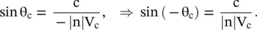

Figure 5.15 Cerenkov radiation in DPS and DNG media.
Figure (5.15d)shows that the wavevectors  and Poynting vectors
  , for both the upper and lower radiations, are anti‐parallel that causes the backward radiation. Thus, a DNG medium supports the reverse, i.e. inverse Cerenkov radiation. The metamaterial medium could be continuously varied from the DPS to DNG forming the forward end‐fire to broadside to backward end‐fire antenna [J.26, J.27, B.6, B.7]. The inverse Cerenkov radiation has been experimentally confirmed in the microwave frequency range [J.28]. The realization of such a microstrip antenna is illustrated in the subsection (22.4.1) of chapter 22.
5.5.8 Metamaterial Perfect Absorber (MPA)
The absorbing materials are needed to absorb undesired reflected EM‐waves and interfering signals. The perfect absorbing materials absorb 100% of incident RF power without any reflection , scattering , and transmission . The frequency‐dependent absorbed power A(ω), i.e. attenuation , of an absorber, in absence of scattering and diffraction, is expressed as
(5.5.43) 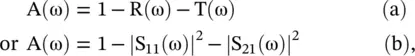
where R(ω) is the reflectivity (reflectance) related to the reflection coefficient (S 11) and T(ω) is the transmissivity (transmittance) of the absorbing sheet [B.14]. The attenuation A(ω) is also called absorptivity (absorptance). For 100% absorption, both R(ω) and T(ω) must be zero. To get R(ω) = 0, the absorbing sheet must be matched to the free space impedance η 0= 377 Ω over a frequency band and for getting T(ω) = 0 the absorbed power must be dissipated in the absorbing sheet. The transmissivity can be made zero even by placing a conducting sheet behind the absorbing sheet. However, it may result in multiple reflections degrading R(ω) [J.29].
Salisbury Absorber
The classical Salisbury absorber , shown in Fig (5.16a), is a narrow band resonant type absorber. The absorbing resistive screen has resistive 377Ω/sq impedance so that it is matched to free space. A metallic sheet ( electric‐wall ) placed behind the absorbing screen at a distance λ 0/4 creates the magnetic‐wall , i.e. the high impedance surface (HIS) at the plane of the resistive screen. The equivalent transmission line model of free space shows the absorbing screen as a 377Ω load followed by an open‐circuited termination corresponding to the magnetic‐wall. The concept of magnetic‐wall is discussed in the subsection (7.2.2) of chapter 7. At the magnetic‐wall, the total tangential components of the incident and reflected waves provide a high‐intensity electric field, i.e. 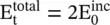 . However, the total tangential component of the magnetic field is zero, i.e.
  . The total electric field induces a current on the resistive screen placed at the magnetic‐wall. The absorbed incident RF power is dissipated. Salisbury absorbing sheet is narrowband, thick, and bulky. By placing several absorbing resistive screens above the conducting plane, over a distance λ 0, a broadband absorber, known as Jaumann absorber , is obtained [B.15]. Again, it is a thick and bulky absorber. The metasurface provides an alternate arrangement for creating the high impedance surface to develop a thin and compact absorber. The realization of the metasurface is discussed in section (22.5) of chapter 22.
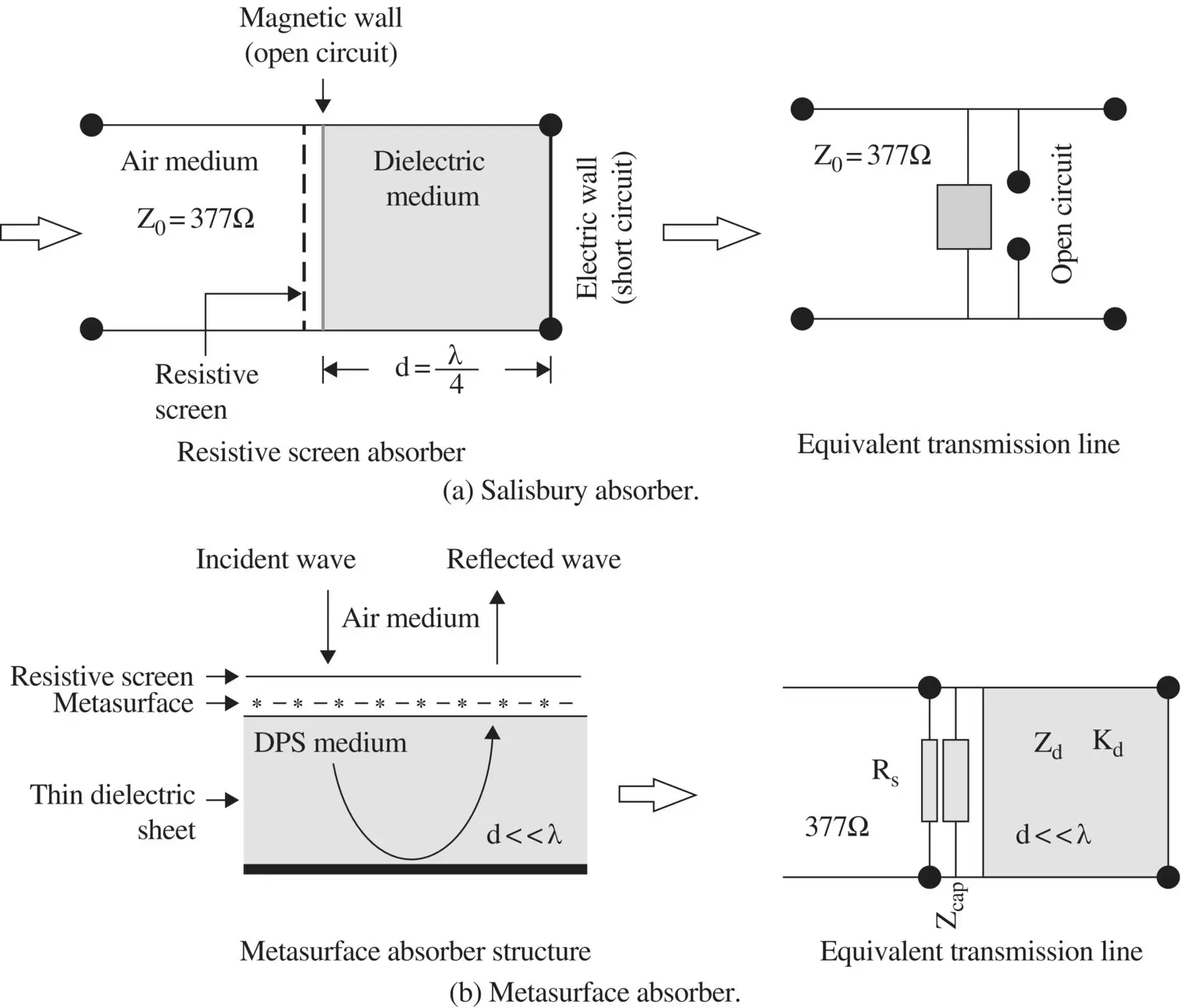
Figure 5.16 Composite surface absorber.
Metasurface Absorber
Figure (5.16b)shows the composition of the metasurface‐based absorber [J.30, J.31]. A thin dielectric sheet d < < λ 0is backed by a conducting surface. An inductive surface is created at the dielectric surface. The capacitive grid of lines or patches is constructed on the dielectric surface such that the surface resonance creates the metasurface, i.e. the high impedance surface at the plane of the air‐dielectric interface. Like a Salisbury absorber, again 377 Ω/sq resistive screen is placed at the interface to get the impedance matching with free space. The absorbed RF power is dissipated as heat.
Читать дальшеИнтервал:
Закладка:
Похожие книги на «Introduction To Modern Planar Transmission Lines»
Представляем Вашему вниманию похожие книги на «Introduction To Modern Planar Transmission Lines» списком для выбора. Мы отобрали схожую по названию и смыслу литературу в надежде предоставить читателям больше вариантов отыскать новые, интересные, ещё непрочитанные произведения.


Обсуждение, отзывы о книге «Introduction To Modern Planar Transmission Lines» и просто собственные мнения читателей. Оставьте ваши комментарии, напишите, что Вы думаете о произведении, его смысле или главных героях. Укажите что конкретно понравилось, а что нет, и почему Вы так считаете.