Perovskite Materials for Energy and Environmental Applications
Здесь есть возможность читать онлайн «Perovskite Materials for Energy and Environmental Applications» — ознакомительный отрывок электронной книги совершенно бесплатно, а после прочтения отрывка купить полную версию. В некоторых случаях можно слушать аудио, скачать через торрент в формате fb2 и присутствует краткое содержание. Жанр: unrecognised, на английском языке. Описание произведения, (предисловие) а так же отзывы посетителей доступны на портале библиотеки ЛибКат.
- Название:Perovskite Materials for Energy and Environmental Applications
- Автор:
- Жанр:
- Год:неизвестен
- ISBN:нет данных
- Рейтинг книги:5 / 5. Голосов: 1
-
Избранное:Добавить в избранное
- Отзывы:
-
Ваша оценка:
Perovskite Materials for Energy and Environmental Applications: краткое содержание, описание и аннотация
Предлагаем к чтению аннотацию, описание, краткое содержание или предисловие (зависит от того, что написал сам автор книги «Perovskite Materials for Energy and Environmental Applications»). Если вы не нашли необходимую информацию о книге — напишите в комментариях, мы постараемся отыскать её.
The book provides a state-of-the-art summary and discussion about the recent progress in the development and engineering of perovskite solar cells materials along with the future directions it might take.
Audience
Perovskite Materials for Energy and Environmental Applications — читать онлайн ознакомительный отрывок
Ниже представлен текст книги, разбитый по страницам. Система сохранения места последней прочитанной страницы, позволяет с удобством читать онлайн бесплатно книгу «Perovskite Materials for Energy and Environmental Applications», без необходимости каждый раз заново искать на чём Вы остановились. Поставьте закладку, и сможете в любой момент перейти на страницу, на которой закончили чтение.
Интервал:
Закладка:
From the optical perspective, in order to achieve greater light conversion efficiencies, both the effective use of solar spectrum and light distribution in the solar cells are significant. Light regulation is accomplished in thin film solar cells through the application of techniques for light trapping. The techniques for trapping of light are focused on substrates with textured surface being introduced and using special (back-) reflector layers. The substrates with textured surface provide rough interfaces to the solar cells. The light incident at rough interfaces is scattered and the simulation of solar cells must consider the rough interface scattering mechanisms so as to precisely assess the generation profile for charge carriers within the solar cell. It needs the design of optical models which take into account propagation of both coherent nonscattered (specular) light and incoherent distributed (diffused) light through a system.
To use the solar spectrum efficiently, a multi-junction approach is required in thin-film silicon solar cells. At an interface between two neighbouring junctions, the tunnelling assisted recombination is accountable for the movement of the charge carriers through a solar cell with several junctions. Such an interface is defined as the tunnel-recombination junction (TRJ). Two methods can be used for modeling TRJ in the ASA program. The Delft approach utilizes the improved transport of carriers in the high-field region of TRJ and the trap-assisted tunnelling model. The Pennsylvania approach utilizes the implementation of a strongly defective layer with a sharply compact bandgap at the interface of n/p and the gradation of the n-layer and p-layer mobility gap in the regions next to the defective layer.
The ASA program’s key characteristics are outlined [4]:
Amorphous and/or crystalline multilayer semiconductor device modeling
Models including both the extended and the localized (tail and defect) state that describe a complete DOS as an energy function.
Use of the defect-pool model for the distribution of defectstates in a-Si:H
Basic statistics for generation-recombination of donor and acceptor states and of ambipolar states
Optical models for measuring the absorption profile in flat and/or rough interfaces
Constant adjustment (gradation) of virtually all input parameters as a function of position in the device or in the gap energy level
Tunnel-recombination junction model
a-Si:H solar cell degradation modeling
Written in language ANSI C
The ASA program can be installed on computers working under Windows or Linux operating systems. The ASA program is protected against unauthorised use and therefore its operation is allowed only with the simultaneous use of the ASA protection key [5–7].
Here, one calculation using the ASA program is followed on the basis of the flowchart in Figure 1.2[3, 8–12]:
1 The ASA program has a built-in parser to run through the input file. After one statement is read, the appropriate part of the program is invoked.
2 The first part of an input file always consists of statements thatDefine the simulated device, i.e. the layers, including their width and the grid.Set electrical parameters of the material, e.g., the valance tail slope parameters Nv0, Evo. These parameters are set for every electrical layer.Set optical parameters, e.g., the refractive index and extinction coefficient of the layers.Set calculation and model settings, e.g., if the Newton method is to be used.
3 After this initialization, the calculations are started with “solve.”The program generates the grid according to the definition earlier in the input file. The arrays of the simulated device are allocated and filled with the (initial) values defined by the given (electrical) parameters. When the defect pool model is selected, the defect density NDB(x) is calculated.If it is not read from external file, the program calculates the generation rate in the device using the GENPRO1, GENPRO2, or GENPRO3 module.One of the five simulation modes can be selected by a “solve” statement:(a) equil: in this mode, the electron, hole densities and the matching potential are calculated in thermodynamic equilibrium. These calculations are automatically carried out before mode 2.(b) jv: the current-voltage characteristics of the simulated device are computed, by using the Poisson and continuity equations. A selection can be made between the Newton and Gummel method. The calculations can be carried out with or without carriers generation by illumination.(c) cv: the capacitance-voltage characteristics of the simulated device are calculated. It is calculated by using mode 2 to find the currents at an applied voltage of and , which gives rise to a difference in charge density Δρ(x). By calculating the difference in surface charge at the front and back contacts, Δσ is also found. These define the capacitance at voltage V.(d) sr: the spectral response (i.e. the external quantum efficiency EQE) is calculated by using mode 2 and the generation rate profile calculated by one of the optical models. The EQE is defined by ΔI/(qΔnphoton), where Δnphoton is the differential number of photons between the (optional) bias spectrum S and the bias spectrum plus a monochromatic probe light S + Δnphoton.(e) rt: the reflection and transmission are calculated. This is carried out by module GENPRO1 (no scattering included).
4 The desired program output can finally be saved to particular files using the “print” statement.
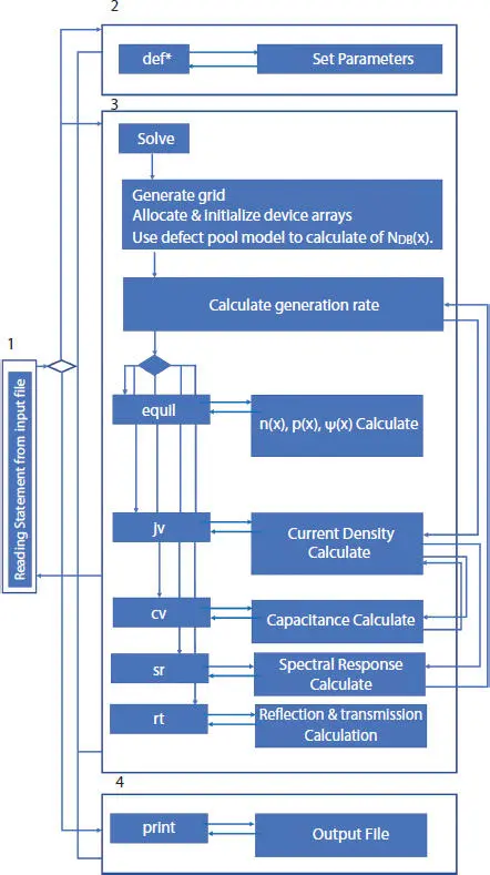
Figure 1.2 Flowchart showing steps for calculation using ASA adapted from [3].
1.4 Analysis of Microelectronic and Photonic Structures (AMPS)
AMPS is a computer-based program in one-dimensional designed to simulate physics of transport in solid-state semiconductor devices. This applies the first principles of continuity equations and Poisson’s equations method to examine transport behavior of electronic and optoelectronic semiconductor device based structures. Such architectures of device can consist of or incorporate amorphous or crystalline, polycrystalline materials. AMPS numerically solve the three controlling equations for semiconductor devices (the Poisson equation, the equations of electron continuity, and the hole continuity) short of having any a-priori statements regarding the processes of regulation of transport in such devices. AMPS can be used with this general and precise numerical treatment to study various device structures, including the following [13]:
Solar cells having P-n and p-i-n structures and detectors with homojunction and heterojunction;
Homojunction and heterojunction of microelectronic structures of p-n, p-i-n, n-i-n and p-i-p;
Designs of solar cells with multijunction;
Microelectronic multi-junction structures;
Structures for detectors with graded composition and solar cells;
Microelectronic structures graded in composition;
New microelectronic, photovoltaic and optoelectronic devices;
Optional back layered Schottky barrier devices.
Information, such as J-V characteristics, can be achieved in the dark and under illumination using the solutions given by an AMPS simulation software. These can be measured as a temperature variable. Collection efficiencies can also be obtained for solar cell, as well as detector designs as a function of light bias, voltage, and temperature. Additionally, significant information, like electric field concentrations, free and trapped carrier populations, profiles of recombination, and current densities of individual carriers, can be found from the AMPS program as a function of position. AMPS can be used to evaluate transport in different types of device structures that may include amorphous, crystalline, or polycrystalline layers or combinations of these. AMPS is intended to analyze, model, and optimize microelectronic, photovoltaic, or optoelectronic device architectures.
Читать дальшеИнтервал:
Закладка:
Похожие книги на «Perovskite Materials for Energy and Environmental Applications»
Представляем Вашему вниманию похожие книги на «Perovskite Materials for Energy and Environmental Applications» списком для выбора. Мы отобрали схожую по названию и смыслу литературу в надежде предоставить читателям больше вариантов отыскать новые, интересные, ещё непрочитанные произведения.


Обсуждение, отзывы о книге «Perovskite Materials for Energy and Environmental Applications» и просто собственные мнения читателей. Оставьте ваши комментарии, напишите, что Вы думаете о произведении, его смысле или главных героях. Укажите что конкретно понравилось, а что нет, и почему Вы так считаете.