Perovskite Materials for Energy and Environmental Applications
Здесь есть возможность читать онлайн «Perovskite Materials for Energy and Environmental Applications» — ознакомительный отрывок электронной книги совершенно бесплатно, а после прочтения отрывка купить полную версию. В некоторых случаях можно слушать аудио, скачать через торрент в формате fb2 и присутствует краткое содержание. Жанр: unrecognised, на английском языке. Описание произведения, (предисловие) а так же отзывы посетителей доступны на портале библиотеки ЛибКат.
- Название:Perovskite Materials for Energy and Environmental Applications
- Автор:
- Жанр:
- Год:неизвестен
- ISBN:нет данных
- Рейтинг книги:5 / 5. Голосов: 1
-
Избранное:Добавить в избранное
- Отзывы:
-
Ваша оценка:
Perovskite Materials for Energy and Environmental Applications: краткое содержание, описание и аннотация
Предлагаем к чтению аннотацию, описание, краткое содержание или предисловие (зависит от того, что написал сам автор книги «Perovskite Materials for Energy and Environmental Applications»). Если вы не нашли необходимую информацию о книге — напишите в комментариях, мы постараемся отыскать её.
The book provides a state-of-the-art summary and discussion about the recent progress in the development and engineering of perovskite solar cells materials along with the future directions it might take.
Audience
Perovskite Materials for Energy and Environmental Applications — читать онлайн ознакомительный отрывок
Ниже представлен текст книги, разбитый по страницам. Система сохранения места последней прочитанной страницы, позволяет с удобством читать онлайн бесплатно книгу «Perovskite Materials for Energy and Environmental Applications», без необходимости каждый раз заново искать на чём Вы остановились. Поставьте закладку, и сможете в любой момент перейти на страницу, на которой закончили чтение.
Интервал:
Закладка:
The electrical characteristics can be determined according to the defined physical structure and conditions of bias. This can be done by the assumption that the device’s function can be approximated into a grid in one dimension composed of a set of grid points also called as nodes. The transport of carriers through the system can be modeled by adding the set of differential equations (Poisson’s equation and continuity equations) on this grid (or the discretization of the equation). The grid with finite element can be used to depict the domain of the simulation.
SCAPS is a program for Windows, and some of its chief characteristics are classified here as follows:
It is possible to include up to seven layers of semiconductor to the solar cell device.
When required, gradation of nearly all physical parameters can be done in a new window.
Capacity to approximate band diagram in steady state, profile for recombination, and transport of carrier.
Variable bias of voltage, different temperature, and various illumination options
Can be used to measure concentrations and currents, J-V, C-f, C-V, and Q-V, AC characteristics and spectral response.
Calculation of single and batch values.
Final, as well as intermediate values, graphs, and other significant data, can be obtained as output and can be exported
SCAPS are arranged in several panels where the parameters can be defined by the user. The key panel is the “action panel” ( Figure 1.3), in which one can set an operation point (temperature, voltage, frequency, and illumination) and the action list for calculation to be performed (J-V, C-f, C-V, Q(λ)). The running parameter (V, f, or λ) vary in the definite range in each calculation, whereas the values quantified in the operation point are for all other parameters. The user can also view the results earlier calculated directly, i.e., J-V, C-f, C-V, Q(λ), likewise, band diagrams, electric field, densities of the carrier, partial currents of recombination [36–45].
We click on the “set problem” button for the problem definition, i.e., the geometry, materials, and different characteristics of the solar cell. As depicted in Figure 1.4, the Solar Cell Definition Panel opens. In this panel, we can define up to 9 layers of structures. The back contact is the first layer; the last one is the front contact. The properties of intermediate semiconductor layers can be specified by the user. Each layer contains the following semiconductor properties, except for front and back contact:
thickness (μm),
electron affinity (eV),
band gap (eV),
dielectric permittivity (relative),
valance band effective density of states (1/cm3),
conduction band effective density of states (1/cm3),
hole thermal velocity (cm/s),
electron thermal velocity (cm/s),
acceptor shallow density (ND),
donor shallow density (ND).

Figure 1.3 Action panel of SCAPS.

Figure 1.4 Solar cell definition panel of SCAPS.
The optical absorption of the semiconductor layers can be taken from a user file. Examples of such user files are distributed with the program: Si.abs , CdS.abs , GaAs.abs , and so on. We can add other absorption files for other relevant materials.
We can also change the model for absorption, model for recombination, and apply defects to a surface in addition to these basic parameters. A panel for layer properties snapshot is illustrated in Figure 1.5.
On the panel for cell definition, which opens the panel for the properties of contacts ( Figure 1.5), you can configure the contact properties by either selecting the front or back contact button.
The identification of each contact is made as follows:
electron and hole surface recombination velocities,
information about the metal work function.
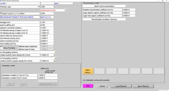
Figure 1.5 Layer properties panel in SCAPS.
After loading the solar cell design with the button for set problem on SCAPS, one can set the working point. The work point specifies the parameters in a measurement that are not varied:
Temperature, T: appropriate to all measurements. In SCAPS, the only variables that have an explicit dependence on temperature are NC(T), NV(T), and thermal voltage kBT.
Voltage, V: is discarded in simulation of I-V and C-V. It is the voltage for dc-bias in simulation of C-f and simulation of QE(λ). SCAPS starts at 0V and proceeds through a series of steps at the point of operation, which we can also define.
Frequency, f: is discarded in simulation of I-V, QE(λ) and C-f. It is the frequency of the simulation of the C-V measurement.
Illumination, the illumination requirements can be further defined when simulating under illumination. The main options are: dark or light, light side choice (left/right), spectrum option. A single sun(=1000 W/m3) illumination with the “air mass.5, global” spectrum is the default, but for specialized simulations, we have a wide range of monochromatic light and spectra.
In a diode, the current at n-contact is converted from the p-contact hole current to the electron current. It implies that recombination must occur somewhere in the diode, even in the most ideal device. The user must define recombination at least at one location (in a layer or interface) somewhere. Defects are most important parameters for study of solar cells. The following parameters identify defects in SCAPS:
position of energy level in the gap,
type of defect (i.e. acceptor, donor or neutral),
thermal capture cross-section for electrons,
thermal capture cross-section for holes,
energetic distribution (single, uniform …),
defect energy level reference (above EV or below EC),
optical cross section of electrons,
capture cross section of holes,
concentration of defects.
We can select one or more of the following measurements to be simulated in the action part of the action panel ( Figure 1.3): I-V, C-V, C-f and QE(λ). The start and end values of the argument and the number of steps can be adjusted if necessary.
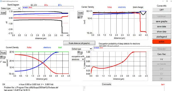
Figure 1.6 Screenshot of energy bands panel window in SCAPS.
We select the “calculate” button in the action panel after implementing all the necessary data (layer properties, solar cell configuration). The panel of the energy bands opens, and the calculations begin. The window for panel for energy bands opens after measurement with the band diagram, density of carriers, density of current, and probability of occupation of deep defects of graph plots of electrons as shown in Figure 1.6.
Then from the right side of the screen window of the energy bands one can select choices (Gen-Rec, I-V). The behavior of the solar cell like the short circuit current (J SC) may be derived from the I-V curve. The results can be saved for further editing or use in other programs as ASCII files (e.g., Excel). It is broadly used for the simulation and analysis of different types of solar cells [46–49].
Читать дальшеИнтервал:
Закладка:
Похожие книги на «Perovskite Materials for Energy and Environmental Applications»
Представляем Вашему вниманию похожие книги на «Perovskite Materials for Energy and Environmental Applications» списком для выбора. Мы отобрали схожую по названию и смыслу литературу в надежде предоставить читателям больше вариантов отыскать новые, интересные, ещё непрочитанные произведения.


Обсуждение, отзывы о книге «Perovskite Materials for Energy and Environmental Applications» и просто собственные мнения читателей. Оставьте ваши комментарии, напишите, что Вы думаете о произведении, его смысле или главных героях. Укажите что конкретно понравилось, а что нет, и почему Вы так считаете.