Perovskite Materials for Energy and Environmental Applications
Здесь есть возможность читать онлайн «Perovskite Materials for Energy and Environmental Applications» — ознакомительный отрывок электронной книги совершенно бесплатно, а после прочтения отрывка купить полную версию. В некоторых случаях можно слушать аудио, скачать через торрент в формате fb2 и присутствует краткое содержание. Жанр: unrecognised, на английском языке. Описание произведения, (предисловие) а так же отзывы посетителей доступны на портале библиотеки ЛибКат.
- Название:Perovskite Materials for Energy and Environmental Applications
- Автор:
- Жанр:
- Год:неизвестен
- ISBN:нет данных
- Рейтинг книги:5 / 5. Голосов: 1
-
Избранное:Добавить в избранное
- Отзывы:
-
Ваша оценка:
Perovskite Materials for Energy and Environmental Applications: краткое содержание, описание и аннотация
Предлагаем к чтению аннотацию, описание, краткое содержание или предисловие (зависит от того, что написал сам автор книги «Perovskite Materials for Energy and Environmental Applications»). Если вы не нашли необходимую информацию о книге — напишите в комментариях, мы постараемся отыскать её.
The book provides a state-of-the-art summary and discussion about the recent progress in the development and engineering of perovskite solar cells materials along with the future directions it might take.
Audience
Perovskite Materials for Energy and Environmental Applications — читать онлайн ознакомительный отрывок
Ниже представлен текст книги, разбитый по страницам. Система сохранения места последней прочитанной страницы, позволяет с удобством читать онлайн бесплатно книгу «Perovskite Materials for Energy and Environmental Applications», без необходимости каждый раз заново искать на чём Вы остановились. Поставьте закладку, и сможете в любой момент перейти на страницу, на которой закончили чтение.
Интервал:
Закладка:
We can derive an expression for the concentration of holes in a similar manner. The probability that a state of energy is captured by a hole is the same as its not being held by an electron, i.e., 1-f(E). Thus,
(1.7) 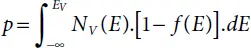
Applying the Boltzmann approximation, we can get:
(1.8) 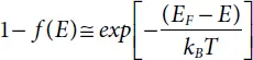
Substituting Equations 1.1(b)and 1.8into Eq. 1.7yields
(1.9) 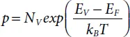
(1.10) 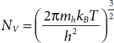
NV shows the valance band effective density of states. The difference in the values of NC and NV is only because of the difference in me and mh . The variation in NC and NV from one semiconductor to another is also due to the dissimilarity in the effective masses, also.
Intrinsic carrier concentration
The number of electrons present in the conduction band and the number of holes present in the valance band are equal in an intrinsic (undoped) semiconductor which is in thermal equilibrium; n = p = ni , where ni is the concentration of carriers of intrinsic semiconductors.
When multiplying the corresponding sides of Equations 1.5and 1.9one obtains:
(1.11) 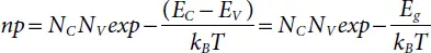
where Eg is the forbidden gap:
(1.12) 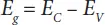
Equation 1.11shows that for a given semiconductor and T the product of np is a constant, free of the concentrations of the dopant. It is a significant relation and is generally shown in the following form:
(1.13) 
(1.14) 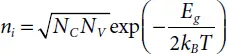
The equation 1.13is called law of mass action and it is true for any semiconductor at equilibrium. The intrinsic carrier concentration in a semiconductor is dependant only on the bandgap Eg . It is a material property (at a given temperature).
When in the intrinsic material we represent the Fermi level position Ei one can obtain from equations 1.5and 1.9:
(1.15) 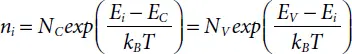
From equation 1.15we can deduce easily the position of Ei , which is given by:
(1.16) 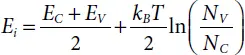
The Fermi level Ei is nearby to the midgap; a minor alteration is due to the variance in the effective densities of conduction and valance and band.
Also using Equation 1.15and reference energy as Ei , we have for N-type materials the alternate equations given as:
(1.17) 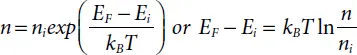
And for P-type materials:
(1.18) 
Donors and acceptors
The number of holes and electrons in their bands respectively and therefore the conductivity of the semiconductor, may be regulated by adding different dopants or different types of impurities called acceptors and donors. The doped semiconductor, known as extrinsic material.
A semiconductor has four kinds of charged species: holes, electrons, donor ions which are positive Nd , and acceptor ions which are negative Na . Generally, there is no net charge in all samples.
The densities of the negative and positive particles should be equal in order to maintain the charge neutrality:
(1.19) 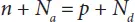
For n and p we can solve equations 1.19and 1.13:
(1.20a) 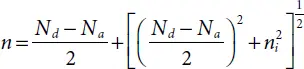
(1.20b) 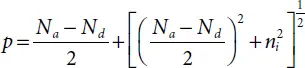
The equations 1.20aand 1.20bare seldom used. Alternatively, either of the following cases is mostly valid:
1 Nd – Na ≫ ni (i.e., N-type material),(1.21)(1.22)If additionally, Nd ≫ Na, then(1.23)The Fermi energy can then be written as:(1.24)
2 Na – Nd ≫ ni (i.e., P-type material)(1.25)(1.26)If furthermore, Na ≫ Nd, then(1.27)The Fermi energy can then be written as:(1.28)
B. Nonequilibrium carrier concentration
Many semiconductor devices work by producing charge carriers that exceed the thermal equilibrium values, such excess carriers can be generated either by optical excitation or by adding an electrical field.
Through producing excess carriers (electrons and holes), thermal equilibrium in the semiconductor is no longer maintained, and the Fermi energy is no longer strictly specified. For the nonequilibrium semiconductor, we can outline two novel parameters: the quasi-Fermi energy for electrons and holes respectively.
The electron and hole concentrations of for the nonequilibrium are then given by:
(1.29) 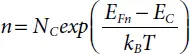
(1.30) 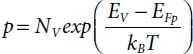
EFn and EFp are the quasi-Fermi levels for electron and hole.
When electrons and holes are at equilibrium, EFn and EFp coincide and this is known as EF .
(II) Basic equations for semiconductor modeling
The so-called equations of semiconductor devices could explain the activity of most of the devices made up of semiconductor materials, including solar cells.
Читать дальшеИнтервал:
Закладка:
Похожие книги на «Perovskite Materials for Energy and Environmental Applications»
Представляем Вашему вниманию похожие книги на «Perovskite Materials for Energy and Environmental Applications» списком для выбора. Мы отобрали схожую по названию и смыслу литературу в надежде предоставить читателям больше вариантов отыскать новые, интересные, ещё непрочитанные произведения.


Обсуждение, отзывы о книге «Perovskite Materials for Energy and Environmental Applications» и просто собственные мнения читателей. Оставьте ваши комментарии, напишите, что Вы думаете о произведении, его смысле или главных героях. Укажите что конкретно понравилось, а что нет, и почему Вы так считаете.