Perovskite Materials for Energy and Environmental Applications
Здесь есть возможность читать онлайн «Perovskite Materials for Energy and Environmental Applications» — ознакомительный отрывок электронной книги совершенно бесплатно, а после прочтения отрывка купить полную версию. В некоторых случаях можно слушать аудио, скачать через торрент в формате fb2 и присутствует краткое содержание. Жанр: unrecognised, на английском языке. Описание произведения, (предисловие) а так же отзывы посетителей доступны на портале библиотеки ЛибКат.
- Название:Perovskite Materials for Energy and Environmental Applications
- Автор:
- Жанр:
- Год:неизвестен
- ISBN:нет данных
- Рейтинг книги:5 / 5. Голосов: 1
-
Избранное:Добавить в избранное
- Отзывы:
-
Ваша оценка:
Perovskite Materials for Energy and Environmental Applications: краткое содержание, описание и аннотация
Предлагаем к чтению аннотацию, описание, краткое содержание или предисловие (зависит от того, что написал сам автор книги «Perovskite Materials for Energy and Environmental Applications»). Если вы не нашли необходимую информацию о книге — напишите в комментариях, мы постараемся отыскать её.
The book provides a state-of-the-art summary and discussion about the recent progress in the development and engineering of perovskite solar cells materials along with the future directions it might take.
Audience
Perovskite Materials for Energy and Environmental Applications — читать онлайн ознакомительный отрывок
Ниже представлен текст книги, разбитый по страницам. Система сохранения места последней прочитанной страницы, позволяет с удобством читать онлайн бесплатно книгу «Perovskite Materials for Energy and Environmental Applications», без необходимости каждый раз заново искать на чём Вы остановились. Поставьте закладку, и сможете в любой момент перейти на страницу, на которой закончили чтение.
Интервал:
Закладка:
This book provides a state-of-the-art summary and discussion about the recent progress in the development and engineering of PSCs materials along with the future directions it might take. Moreover, the recent advances in perovskite materials for energy conversion and environmental applications have been compiled herein.
Khursheed Ahmad
Waseem Raza
April 2022
1
Computational Approach for Synthesis of Perovskite Solar Cells
A.S. Mathur* and B.P. Singh
Department of Physics, Institute of Basic Science, Dr. Bhimrao Ambedkar University, Agra (U.P.), India
Abstract
Computational approach has emerged as an effective technique for analyzing the synthesis of novel structures of perovskite solar cells. This approach involves modeling and simulation of solar cells. With respect to solar cells, numerical simulation has proven to be a viable tool over the years to study and comprehend the features and properties of solar cell devices, like the electrical, optical, and mechanical properties of complicated device structures of solar cell. The advantages of simulation are calculating the electrical behavior before the manufacturing process, calculating and visualizing internal electronic values that cannot be measured. It also helps to reduce processing costs and time spent on manufacturing solar cell devices by providing useful information on how the parameters of production can be varied to improvise the behavior of the device. Quantitative modeling of the photovoltaic response of the solar cell is an important subject for improving both the understanding of operation mechanisms and the device performance. In the present chapter, basic steps involved in the modeling of solar cells have been described along with some simulation approaches being used for perovskite solar cells, such as SCAPS-1D, AMPS, ASA, AFORS-HET, and so on. Results of some recent studies have also been presented, elucidating the importance of modeling and simulation approaches in the design and development of perovskite solar cells.
Keywords:Perovskite solar cells, modeling, simulation, photovoltaic parameters
1.1 Introduction
Computational simulation is a technique that uses a software program to research and analyze the behavior of a real device or an imaginary system. Simulation is based on a mathematical model describing the process under study. In many instances of functional interest, numerical simulation of semiconductor devices is an effective tool for chip development. It is a significant technique for optimizing new semiconductor devices.
With respect to solar cells, numerical simulation has proven to be a viable tool over the years to study and comprehend the features and properties of solar cell devices, like the electrical, optical, and mechanical properties of complicated device structures of solar cell. The advantages of simulation are calculating the electrical behavior before the manufacturing process, calculating and visualizing internal electronic values that cannot be measured. It also helps to reduce processing costs and time spent on manufacturing solar cell devices by providing useful information on how the parameters of production can be varied to improvise the behavior of the device.
In this chapter, different simulation softwares are discussed. It presents the physical basis for modeling of semiconductor devices. Basic equations required for semiconductor modeling are also given here. Then after, it discusses in detail various recombination phenomenon taking place in semiconductors. After this, some softwares used for simulation of different types of solar cells are detailed one by one.
1.2 Preliminary Steps
(I) Physical Basis for Semiconductor Device Modeling
A. Semiconductor at Thermal Equilibrium
Every operation of a semiconductor device relies on the carriers carrying charge within the semiconductor and creating electrical currents. It is crucial to understand the exact number of these carriers so as to interpret the functioning of the device. First, we assume the thermal equilibrium of the semiconductor. This means that there are no external forces acting on the semiconductor, such as voltage, electrical fields, magnetic fields, or temperature gradients. In this case, all of the semiconductor’s properties are independent of time [1].
Carrier Concentration
First, we consider the intrinsic condition applied to the semiconductor without any impurities. The current in a semiconductor is contributed by two types of charge carrier, the electron and the hole. To evaluate the carrier concentration the function of the density of the allowed electron energy states and the occupation function of the allowed energy states must be established. The function of energy density states, N(E) , defines the number of allowed electronic states per unit volume and energy. The function describing occupation is the well-established distribution function given by Fermi-Dirac, f(E) , which defines the ratio of filled states having an electron to maximum states allowed with the given energy E.
The density of states at an energy E in the conduction band, which is given as NC(E) is close to EC , and in the valance band, NV(E) is close to EV and are given by [2]:
(1.1a) 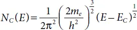
(1.1b) 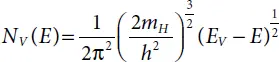
with me and mh being electron and hole effective mass respectively. EC denotes the conduction band bottom, whereas EV represents the valance band top.
The Fermi-Dirac distribution function is expressed as follows:
(1.2) 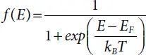
with kB representing the Boltzmann constant, the absolute temperature is represented by T and EF the Fermi energy level.
For energy much greater than kBT (i.e. E – EF ≫ kBT ), the Fermi function can be approximated by the Boltzmann function:
(1.3) 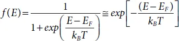
The density of free electrons (n) (conduction-band levels which have been occupied) is found after multiplying the total number of states NC(E) with occupation function f(E) and then integrating over the conduction band:
(1.4) 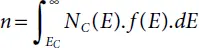
By replacing equations 1.1(a)and 1.3into 1.4the resultant expression for n is found after resolving the equation:
(1.5) 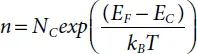
The parameter NC is termed the conduction band effective density of states which is:
(1.6) 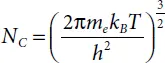
Интервал:
Закладка:
Похожие книги на «Perovskite Materials for Energy and Environmental Applications»
Представляем Вашему вниманию похожие книги на «Perovskite Materials for Energy and Environmental Applications» списком для выбора. Мы отобрали схожую по названию и смыслу литературу в надежде предоставить читателям больше вариантов отыскать новые, интересные, ещё непрочитанные произведения.


Обсуждение, отзывы о книге «Perovskite Materials for Energy and Environmental Applications» и просто собственные мнения читателей. Оставьте ваши комментарии, напишите, что Вы думаете о произведении, его смысле или главных героях. Укажите что конкретно понравилось, а что нет, и почему Вы так считаете.