Perovskite Materials for Energy and Environmental Applications
Здесь есть возможность читать онлайн «Perovskite Materials for Energy and Environmental Applications» — ознакомительный отрывок электронной книги совершенно бесплатно, а после прочтения отрывка купить полную версию. В некоторых случаях можно слушать аудио, скачать через торрент в формате fb2 и присутствует краткое содержание. Жанр: unrecognised, на английском языке. Описание произведения, (предисловие) а так же отзывы посетителей доступны на портале библиотеки ЛибКат.
- Название:Perovskite Materials for Energy and Environmental Applications
- Автор:
- Жанр:
- Год:неизвестен
- ISBN:нет данных
- Рейтинг книги:5 / 5. Голосов: 1
-
Избранное:Добавить в избранное
- Отзывы:
-
Ваша оценка:
Perovskite Materials for Energy and Environmental Applications: краткое содержание, описание и аннотация
Предлагаем к чтению аннотацию, описание, краткое содержание или предисловие (зависит от того, что написал сам автор книги «Perovskite Materials for Energy and Environmental Applications»). Если вы не нашли необходимую информацию о книге — напишите в комментариях, мы постараемся отыскать её.
The book provides a state-of-the-art summary and discussion about the recent progress in the development and engineering of perovskite solar cells materials along with the future directions it might take.
Audience
Perovskite Materials for Energy and Environmental Applications — читать онлайн ознакомительный отрывок
Ниже представлен текст книги, разбитый по страницам. Система сохранения места последней прочитанной страницы, позволяет с удобством читать онлайн бесплатно книгу «Perovskite Materials for Energy and Environmental Applications», без необходимости каждый раз заново искать на чём Вы остановились. Поставьте закладку, и сможете в любой момент перейти на страницу, на которой закончили чтение.
Интервал:
Закладка:
At x distance from the surface of the semiconductor the generation rate G ( x , ν) of electron-hole pairs can be obtained as:
(1.51) 
Where R is the reflectance.
Here an assumption is made that one electron-hole pair is generated by each absorbed photon.
(III) Recombination phenomenon in semiconductors
Recombination is a course of annihilation or destruction of holes and electrons.
There are different mechanisms of recombination significant in the solar cell operation: band-to-band recombination or radiative recombination, Auger recombination, and recombination via defects or traps in the bandgap (often mentioned as Shockley-Read-Hall recombination or SRH). These processes are illustrated if Figure 1.1.
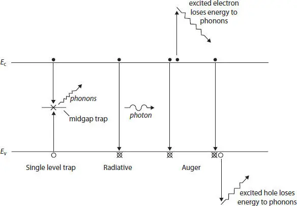
Figure 1.1 The different recombination processes in semiconductors.
A. Radiative recombination
Radiative recombination may be understood as the opposite of optical generation. This recombination takes place if a free electron drops out of the conduction band and recombine with a free hole in the valance band and a photon of energy equivalent to the difference in starting and ending energy states is released. For direct bandgap semiconductors, radiative recombination is very significant, but not as relevant for indirect semiconductors such as silicon, since a photon must also be absorbed or expelled for an electron to complete the transmission.
Due to radiative processes the net recombination rate is expressed as:
(1.52) 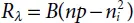
Where B is a material constant.
For n-type semiconductors under low injection ( p 0≤ p ≪ n 0) the net rate of recombination can be given as:
(1.53) 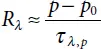
The effective lifetime due to radiative recombination, τλ,p , is given by:
(1.54) 
B. Auger recombination
Auger recombination process is relatively similar to the process of radiative recombination with the exception that the transitional energy is transferred to an electron or hole that is excited in the respective conduction or valance band ( Figure 1.1). Due to Auger recombination the net recombination is expressed as:
(1.55) 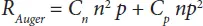
Where Cn and Cp are the electron and hole Auger coefficients, respectively.
The most widely used Auger coefficient values were calculated by Dziewior and Schmid ( Cn = 2.8 × 10 –31 cm 6 s –1and Cp = 0.99 × 10 –31 cm 6 s –1) for Silicon having a doping concentration more than 5 × 10 18 cm –3.
Auger recombination is relevant in semiconductors with high carrier concentration or also under high level injection (e.g. concentrator solar cells).
C. Shockley-Read-Hall recombination (SRH)
The Shockley-Read-Hall recombination process generally occupies the net rate of recombination in low quality materials having high density of defects.
For single-energy level traps the SRH rate of volume recombination, USRH , is expressed as:
(1.56) 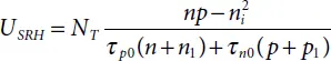
Where τ n0and τ p0are the electron mean carrier lifetime and hole mean carrier lifetime, respectively, and are associated to the charge carrier thermal velocity, v th, the concentration of defect, N T, and the capture cross-sections of electron and capture cross-sections of hole of the specific defect, σ nand σ pas

n 1and p 1are defined as:
(1.57) 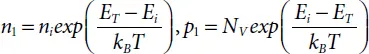
According to definition, n 1and p 1are the free-electron and free-hole concentrations when the Fermi level ( EF ) lies at the trap energy level ( ET ).
Actually, all three recombination processes deliberated here occur simultaneously.
The net recombination can be found by addition of the three rates of recombination as:
(1.58) 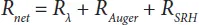
1.3 Advanced Semiconductor Analysis (ASA)
The ASA program is intended to simulate devices based on amorphous and crystalline semiconductors. The ASA program resolves one dimensional elementary semiconductor equations (Poisson equation and electron continuity equation and hole continuity equation) and utilizes variables such as concentration of free electrons, n , and that of holes, p , and electrostatic potential. Additionally, in order to describe explicit device operation and optoelectronic properties of the material it employs several advanced physical.
The ASA one dimensional (1-D) device simulator is very appropriate for simulating thin film structures of silicon solar cells. The program fulfils the usual requirements for simulating thin-film solar cell devices [3].
For modeling silicon thin-film devices the electronic structure of hydrogenated amorphous silicon (a-Si: H) and hydrogenated microcrystalline silicon (μc-Si: H) need to be considered. The atomic structure of a-Si:H shows spatial disorder leading to the energy band gap with edges of conduction band (CB) and valance band (VB) not well-defined with a continuous density of states (DOS). While studying the transport properties of carriers in a-Si:H, in the DOS distribution, it is necessary to differentiate between the localized states and the extended states. Within the mobility gap, the localized states greatly affect the processes of charge trapping followed by recombination. Thus, as is the case with crystalline semiconductor modeling, the charge trapped inside the localized states cannot be neglected. For the calculation of recombination-generation (R-G) statistics different methods are required for the localized states in the mobility gap of a- Si:H as they can be of different nature. The Shockley-Read-Hall (SRH) recombination is not used for amorphous films in device structures in a-Si:H to model recombination as the states introduced by dopants and/or impurities are negligible compared to the recombination via the tail states or dangling bond states. Though, SRH recombination based on the carrier lifetimes can be used for crystalline materials in the ASA program.
Читать дальшеИнтервал:
Закладка:
Похожие книги на «Perovskite Materials for Energy and Environmental Applications»
Представляем Вашему вниманию похожие книги на «Perovskite Materials for Energy and Environmental Applications» списком для выбора. Мы отобрали схожую по названию и смыслу литературу в надежде предоставить читателям больше вариантов отыскать новые, интересные, ещё непрочитанные произведения.


Обсуждение, отзывы о книге «Perovskite Materials for Energy and Environmental Applications» и просто собственные мнения читателей. Оставьте ваши комментарии, напишите, что Вы думаете о произведении, его смысле или главных героях. Укажите что конкретно понравилось, а что нет, и почему Вы так считаете.