Heterogeneous Catalysts
Здесь есть возможность читать онлайн «Heterogeneous Catalysts» — ознакомительный отрывок электронной книги совершенно бесплатно, а после прочтения отрывка купить полную версию. В некоторых случаях можно слушать аудио, скачать через торрент в формате fb2 и присутствует краткое содержание. Жанр: unrecognised, на английском языке. Описание произведения, (предисловие) а так же отзывы посетителей доступны на портале библиотеки ЛибКат.

- Название:Heterogeneous Catalysts
- Автор:
- Жанр:
- Год:неизвестен
- ISBN:нет данных
- Рейтинг книги:4 / 5. Голосов: 1
-
Избранное:Добавить в избранное
- Отзывы:
-
Ваша оценка:
Heterogeneous Catalysts: краткое содержание, описание и аннотация
Предлагаем к чтению аннотацию, описание, краткое содержание или предисловие (зависит от того, что написал сам автор книги «Heterogeneous Catalysts»). Если вы не нашли необходимую информацию о книге — напишите в комментариях, мы постараемся отыскать её.
tate-of-the-art knowledge of heterogeneous catalysts including new applications in energy and environmental fields
This book focuses on emerging techniques in heterogeneous catalysis, from new methodology for catalysts design and synthesis, surface studies and operando spectroscopies, ab initio techniques, to critical catalytic systems as relevant to energy and the environment. It provides the vision of addressing the foreseeable knowledge gap unfilled by classical knowledge in the field.
Heterogeneous Catalysts: Advanced Design, Characterization and Applications
Presents recent developments in heterogeneous catalysis with emphasis on new fundamentals and emerging techniques Offers a comprehensive look at the important aspects of heterogeneous catalysis Provides an applications-oriented, bottoms-up approach to a high-interest subject that plays a vital role in industry and is widely applied in areas related to energy and environment
is an important book for catalytic chemists, materials scientists, surface chemists, physical chemists, inorganic chemists, chemical engineers, and other professionals working in the chemical industry.
Heterogeneous Catalysts — читать онлайн ознакомительный отрывок
Ниже представлен текст книги, разбитый по страницам. Система сохранения места последней прочитанной страницы, позволяет с удобством читать онлайн бесплатно книгу «Heterogeneous Catalysts», без необходимости каждый раз заново искать на чём Вы остановились. Поставьте закладку, и сможете в любой момент перейти на страницу, на которой закончили чтение.
Интервал:
Закладка:
The light absorption of semiconductors is quite different from that in metals due to the electronic band structure in semiconductors. Between the VB and CB of semiconductors, no electron states exist in this energy range called the bandgap. In some semiconductors, the minimal energy state of the CB (conduction band minimum, CBM) and the maximal energy state of the VB (valence band maximum, VBM) are situated in the same crystal momentum in the Brillouin zone (direct gap); in other semiconductors, they are not (indirect gap). There is a slight difference in light absorption between these two types of bandgap structure. But it is not necessary to discuss in this chapter. In general, light absorption of a semiconductor is associated with its bandgap. Semiconductors only absorb photons with the energy equal to or greater than the bandgap. As a result of facets‐dependent anisotropic surface electronic properties that in turn influence the band positions, semiconductor crystals with different dominant facets show shifting in light absorption edges. In applications such as photoelectrochemical catalysis, faceted semiconductors can enhance the light harvesting of photoelectrodes [56–58].
The combination of plasmonic metals and semiconductors with facets engineering has the great potential to adjust the light harvesting for photoelectrodes. For example, the LSPR absorption of the faceted plasmonic metal nanoparticles, such as Au and Pd, can be tuned by embedding them in Cu 2O to form core–shell heterostructure [59–61].
2.4.2 Activity and Selectivity
Numerous studies have shown that catalysts with facets engineering exhibit greater catalytic performance. This exploits one or more unique properties of the well‐defined crystal facets to tune the overall catalytic activity and/or selectivity.
For metal catalysts, activity and selectivity are related to the surface atomic structure of the catalysts, where they can be tuned to enhance effective adsorption and/or promote favorable coordination of adsorbates. These processes are strongly influenced by the arrangement and coordination of surface atoms as well as by the corresponding surface density of states of the different facets. For example, there are two types of flat surfaces of Pt, namely, the Pt{111} facet (hexagonal surface) where each surface atom has six nearest neighbors, and the Pt{100} facet (square surface) where each surface atom has four nearest neighbors. The hexagonal surface is up to seven times more active than the square surface in the aromatization reaction of n ‐heptane to toluene, but the square surface is seven times more active than the hexagonal surface in the alkane isomerization reaction of isobutane to n ‐butane [62]. Also in electrocatalysis, the Pt{210} facet has high activity for electrooxidation of formic acid and electroreduction of CO 2[63]; the Pt{410} facet exhibits high performance in NO decomposition [64]; the Pt{730} shows superior activity in electrooxidation of formic acid and methanol [34].
For the semiconductors in photo‐related catalytic processes, the performance of the faceted semiconductor crystals is affected by the synergetic combination of the intrinsic properties of the bulk and surfaces. A typical photocatalytic process includes the following steps: light absorption of the semiconductor catalyst, excited charges (electrons and holes) generation, excited electrons and holes recombination (bulk and surface), charge migration to the surface, charge trapping at the surface, and transfer to reactants. As such, an ideal semiconductor with good reactivity and selectivity is expected to have a suitable bandgap to absorb the light as much as possible, good separation of charge carriers to avoid the recombination at the bulk and surface, good adsorption of reactants at the surface, fast surface transfer of charge carriers from catalysts to reactants, and suitable CBM and VBM position to provide electron–hole pairs with sufficient redox potentials to catalyze the reactions. Each aspect is affected by one or more properties of the surface and bulk. And these effects are not isolated and may affect one another. Figure 2.6shows how the properties synergistically affect the reactivity and selectivity of semiconductor catalysts and the significance of facets engineering.
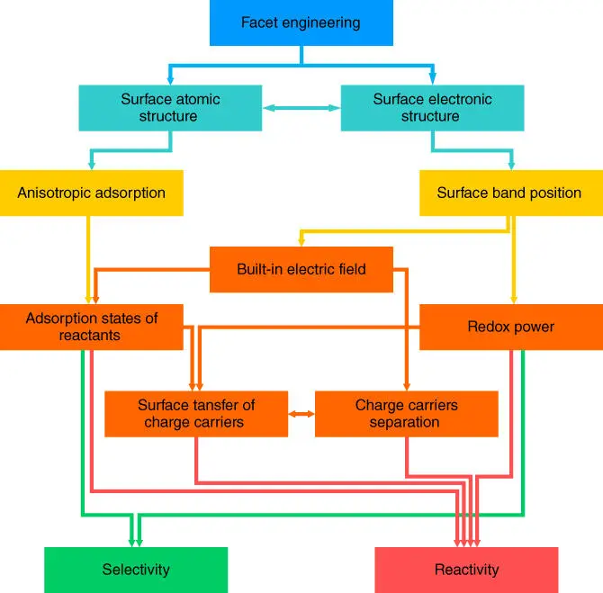
Figure 2.6 Diagram of how the facets engineering affects the selectivity and reactivity of a semiconductor photocatalyst.
2.5 Outlook
Reviewing the published studies of facets engineering, from the faceted crystal synthesis to the investigation of the intrinsic property of the exposed surface and to the overall performance of catalysts in various reactions, it is not difficult to find that the benefits of facets engineering are attributed to crystal anisotropy. Facets engineering itself cannot solve all the issues of catalysts. Although catalytic reactions occur mainly on the surface, there are important inherent bulk properties of the catalysts that play significant roles in concert with the engineered facets to maximize the catalytic performance. Just as in single‐atom catalysis, the substrate has a direct influence on the catalytic atoms. Based on the characteristics of the original catalyst, the morphology control brings more possibilities to the performance of the catalysts.
Although we have attained a good understanding on the mechanisms of facets engineering, we are still facing many challenges, uncertainties, and uncontrollability, such as surface reconstruction. Surface reconstructions always take place on most crystals as a natural phenomenon to minimize surface energy. In many cases where the active facets are the high surface energy facets composed of a high percentage of unsaturated atoms, they become highly unstable upon the removal of capping agents. It inevitably led to the rearrangement of surface atoms or the formation of surface defects, which would have a profound impact on the catalytic properties of the surface.
More efforts need to be dedicated to developing new synthesis methods for new active facets and structure to reveal new facets‐dependent properties and the synergy between these properties and to control surface defects and identify the substantial differences between the ideal and real surface. There is no doubt that facets engineering is an important strategy to promote the performance of catalysts and provides a valuable platform for the rational design and fabrication of efficient material system.
References
1 1 Xia, Y.N., Xiong, Y.J., Lim, B., and Skrabalak, S.E. (2009). Angew. Chem. Int. Ed. 48: 60–103.
2 2 Liu, G., Yang, H.G., Pan, J. et al. (2014). Chem. Rev. 114: 9559–9612.
3 3 Burda, C., Chen, X.B., Narayanan, R., and El‐Sayed, M.A. (2005). Chem. Rev. 105: 1025–1102.
4 4 Pan, J. and Liu, G. (2017). Semicond. Semimet. 97: 349–391.
5 5 Xia, Y.N. and Halas, N.J. (2005). MRS Bull. 30: 338–344.
6 6 Wang, A.Q., Li, J., and Zhang, T. (2018). Nat. Rev. Chem. 2: 65–81.
7 7 Bohme, D.K. and Schwarz, H. (2005). Angew. Chem. Int. Ed. 44: 2336–2354.
8 8 Jiang, H.B., Cuan, Q.A., Wen, C.Z. et al. (2011). Angew. Chem. Int. Ed. 50: 3764–3768.
9 9 Wang, Z.Y., Huang, B.B., Dai, Y. et al. (2012). CrystEngComm 14: 4578–4581.
10 10 Wang, J.H., Yang, T.H., Wu, W.W. et al. (2006). Nanotechnology 17: 719–722.
11 11 Kim, C., Gu, W.H., Briceno, M. et al. (2008). Adv. Mater. 20: 1859–1863.
12 12 Pan, J., Liu, G., Lu, G.M., and Cheng, H.M. (2011). Angew. Chem. Int. Ed. 50: 2133–2137.
13 13 Pan, J., Wu, X., Wang, L.Z. et al. (2011). Chem. Commun. 47: 8361–8363.
Читать дальшеИнтервал:
Закладка:
Похожие книги на «Heterogeneous Catalysts»
Представляем Вашему вниманию похожие книги на «Heterogeneous Catalysts» списком для выбора. Мы отобрали схожую по названию и смыслу литературу в надежде предоставить читателям больше вариантов отыскать новые, интересные, ещё непрочитанные произведения.

Обсуждение, отзывы о книге «Heterogeneous Catalysts» и просто собственные мнения читателей. Оставьте ваши комментарии, напишите, что Вы думаете о произведении, его смысле или главных героях. Укажите что конкретно понравилось, а что нет, и почему Вы так считаете.