Heterogeneous Catalysts
Здесь есть возможность читать онлайн «Heterogeneous Catalysts» — ознакомительный отрывок электронной книги совершенно бесплатно, а после прочтения отрывка купить полную версию. В некоторых случаях можно слушать аудио, скачать через торрент в формате fb2 и присутствует краткое содержание. Жанр: unrecognised, на английском языке. Описание произведения, (предисловие) а так же отзывы посетителей доступны на портале библиотеки ЛибКат.

- Название:Heterogeneous Catalysts
- Автор:
- Жанр:
- Год:неизвестен
- ISBN:нет данных
- Рейтинг книги:4 / 5. Голосов: 1
-
Избранное:Добавить в избранное
- Отзывы:
-
Ваша оценка:
Heterogeneous Catalysts: краткое содержание, описание и аннотация
Предлагаем к чтению аннотацию, описание, краткое содержание или предисловие (зависит от того, что написал сам автор книги «Heterogeneous Catalysts»). Если вы не нашли необходимую информацию о книге — напишите в комментариях, мы постараемся отыскать её.
tate-of-the-art knowledge of heterogeneous catalysts including new applications in energy and environmental fields
This book focuses on emerging techniques in heterogeneous catalysis, from new methodology for catalysts design and synthesis, surface studies and operando spectroscopies, ab initio techniques, to critical catalytic systems as relevant to energy and the environment. It provides the vision of addressing the foreseeable knowledge gap unfilled by classical knowledge in the field.
Heterogeneous Catalysts: Advanced Design, Characterization and Applications
Presents recent developments in heterogeneous catalysis with emphasis on new fundamentals and emerging techniques Offers a comprehensive look at the important aspects of heterogeneous catalysis Provides an applications-oriented, bottoms-up approach to a high-interest subject that plays a vital role in industry and is widely applied in areas related to energy and environment
is an important book for catalytic chemists, materials scientists, surface chemists, physical chemists, inorganic chemists, chemical engineers, and other professionals working in the chemical industry.
Heterogeneous Catalysts — читать онлайн ознакомительный отрывок
Ниже представлен текст книги, разбитый по страницам. Система сохранения места последней прочитанной страницы, позволяет с удобством читать онлайн бесплатно книгу «Heterogeneous Catalysts», без необходимости каждый раз заново искать на чём Вы остановились. Поставьте закладку, и сможете в любой момент перейти на страницу, на которой закончили чтение.
Интервал:
Закладка:
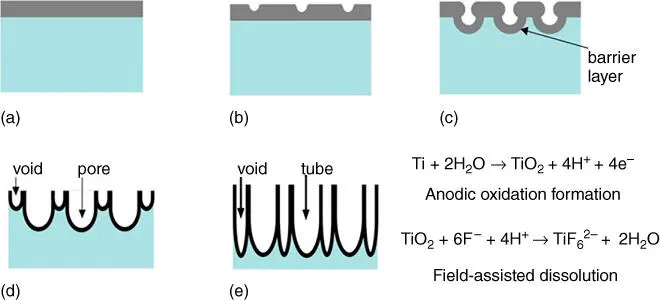
Figure 3.2 Schematic diagram of the growth mechanism for anodized metal foil: (a) growth of thin and compact oxide layer, (b) the initial formation of pores, (c) formation of patterned pores within oxide layer, (d, e) continue growth of the pores to form nanostructures.
As the schematic formation of nanostructure during anodization is explained in Figure 3.2, the presence of those processes can be observed in the measurement of current transient pattern during anodization. Figure 3.3shows a typical transient current profile measured during the reaction under constant applied anodization voltage. The transient current consists of three main stages. In the first stage, the current decays rapidly during the first few minutes of the anodization. At the start of the reaction, electrolyte is in direct contact with the conductive metallic surface, and thus the starting current level is usually high. Under the applied anodization, the oxidation of metallic foil occurs almost instantaneously to form a compact thin oxide surface layer. As the initial oxide layer increases in thickness, so does the electrical resistance of the substrate. As a result, the oxidation of metallic foil slows down, which is reflected by the rapid drop of current density. Sequentially, chemical dissolution of oxide layer by fluoride ion in the electrolyte starts to take place and render more underlayer metal to oxidation; a temporary bounce‐back in current is therefore observed in the second stage. The third stage is the equilibrium stage in which the formation and dissolution of oxide happen at the same competitive rates, reflected by the steady‐state current generation. As the growth of anodic nanostructure is regulated by the formation and dissolution of oxides, the readers can logically expect the important synthetic conditions to be related to the magnitude of applied voltage (strength of oxidation process) and the type or concentration of etching agent (e.g. fluoride ions, which directly influence the strength of dissolution process). Indeed, most of the morphological controls over the anodic oxide thin films are a result of optimal modulation of these two parameters (voltage and electrolyte composition).
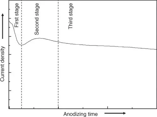
Figure 3.3 Typical current profile under a constant applied anodization voltage of metal foil in organic electrolyte containing fluoride ions.
A number of industrially important metal oxide thin films have been prepared through anodization method such as alumina, silica, and titania. Many more academically interesting simple metal oxide films can be afforded by this method. Figure 3.4shows scanning electron microscopy (SEM) images of metal oxides with anisotropic nanostructures obtained through anodization [20–22]. Some of the most important ones as relevant to catalytic applications include TiO 2and α‐Fe 2O 3nanotubes, Nb 2O 5nanorods, WO 3nanoflowers, and MoO 3truncated rhombohedra. These oxide materials are intrinsic semiconductors with or without nanostructured morphologies, but in the case of the former, their efficiencies as (photo)electrodes can be further augmented. The effect stems from (i) the increased ratio of surface area to volume for electrolyte contact and where reaction takes place, (ii) enhanced light absorption due to trapping of photons within pores, and (iii) the vectorial charge transport.
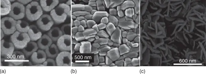
Figure 3.4 SEM images of the simple metal oxides obtained through anodization: (a) titanium dioxide (TiO 2), (b) molybdenum trioxide (MoO 3), and (c) tungsten trioxide (WO 3).
Source: (a) Reprinted with permission from Yun et al. [20]. Copyright 2011, American Chemical Society. (c) Reprinted with permission from Ng et al. [21]. Copyright 2010, American Chemical Society.
The vectorial charge transport is an intriguing phenomenon that relies on the vertically oriented 1D array of the oxide semiconductor and hence deserves special mention here. Under photoexcitation, i.e. when the semiconductor photoanode is exposed to photons with energy equal to or greater than its band gap (see Chapters 11, 31, and 36on the basics of photocatalysis), the generated photoelectrons would need to diffuse to the back of the electrode within its charge carrier lifetime, or they will recombine with the photoholes, hence the loss of photocharge for surface reaction. The photocharge transport can be described by the following equation:
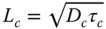
where L cis the diffusion length or distance traveled by the charge carrier (electrons or holes) before recombination, D cis the diffusion coefficient of the charge carrier, and τ cis the lifetime of the charge carrier. It should be noted that the D c(and hence L c) is different for both electron and hole even on the same semiconductor material. For a photoanode (or photocathode) that is composed of irregular‐shaped or randomly packed particles, the photoelectrons (or photoholes) undergo the “random walk motion” that are rarely the most straightforward path to the back of the electrode. With the creation of 1D array of the oxide semiconductor, the diffusion of the photoelectrons is restricted to the shortest vertical path to the back of the electrode. This enables a large fraction of photoelectrons (or photoholes in the case of photocathode) to be collected within their τ c. At the same time, it is important to restrict the wall thickness/diameter to not more than twice the L cof the photoholes (or photoelectrons) such that majority of them could diffuse to the semiconductor surface to catalyze the oxidation (or reduction) reaction. Owing to their advantages, aligned nanotube and nanorod arrays have been used for water photoelectrolysis and the reduction of CO 2.
3.2.1.1 Pulse or Step Anodization
To control the growth of internal channel as mentioned above, a number of strategies external to anodization (dominant by lithography‐based method) have been explored. This includes electron beam lithography, focused ion beam lithography, colloid sphere lithography, and direct laser writing lithography. To search within electrochemical means, pulse or step anodization can offer alternative solutions. This approach is built on the understanding that the development of pore channel can be guided by surface texturization at the initial stage of anodization. Periodic nanostructures are known to grow along the internal channel under anodization. When pulse or step is introduced periodically during anodization, acid anions (such as fluoride ions) are intermittently transported or attracted to the layer near the top of pores. Therefore, compensation of such anions would be established from top to the channel bottom in a periodical manner, which results in the morphological variance of the formed anodic oxide thin film. In literature, it is reported that a low frequency voltage (period τ in minutes) permits the growth of bamboo‐type nanotubes and 2D nanolace sheets of alumina [23], while high frequency current oscillation (period τ in seconds) yields the irregular nanoporous morphology. [24] A more advanced anodization setup involving multiple steps has been explored to precisely control pore channels. Although not yet popular, approaches of changing the type of electrolyte (or concentration) after each step, modulating reaction temperature, and varying the applied voltage or current during anodization have also been explored [25–27]. Although overall aim is to achieve rapid reaction to shorten the catalyst preparation time (industrial's preference), an over‐reactive anodization with ultrafast growth rate can cause concerns, i.e. the physical breaking of nanostructures. Debris of nanotubes has been reported physically lying on the thin films due to the breakage. Unwanted delamination of metal oxide nanostructures from the substrate can happen. Therefore, stabilizing the anodization reaction at ultrafast metal oxide growth rate condition is one of the main aspects in improving the method. Depending on the selected catalytic reaction, amorphous or crystalline structure is desired. As‐anodization thin films usually possess lower degree of crystallinity. Additional crystallization process for the anodized thin film is sometimes needed to suit the targeted catalytic reactions.
Читать дальшеИнтервал:
Закладка:
Похожие книги на «Heterogeneous Catalysts»
Представляем Вашему вниманию похожие книги на «Heterogeneous Catalysts» списком для выбора. Мы отобрали схожую по названию и смыслу литературу в надежде предоставить читателям больше вариантов отыскать новые, интересные, ещё непрочитанные произведения.

Обсуждение, отзывы о книге «Heterogeneous Catalysts» и просто собственные мнения читателей. Оставьте ваши комментарии, напишите, что Вы думаете о произведении, его смысле или главных героях. Укажите что конкретно понравилось, а что нет, и почему Вы так считаете.