Heterogeneous Catalysts
Здесь есть возможность читать онлайн «Heterogeneous Catalysts» — ознакомительный отрывок электронной книги совершенно бесплатно, а после прочтения отрывка купить полную версию. В некоторых случаях можно слушать аудио, скачать через торрент в формате fb2 и присутствует краткое содержание. Жанр: unrecognised, на английском языке. Описание произведения, (предисловие) а так же отзывы посетителей доступны на портале библиотеки ЛибКат.

- Название:Heterogeneous Catalysts
- Автор:
- Жанр:
- Год:неизвестен
- ISBN:нет данных
- Рейтинг книги:4 / 5. Голосов: 1
-
Избранное:Добавить в избранное
- Отзывы:
-
Ваша оценка:
Heterogeneous Catalysts: краткое содержание, описание и аннотация
Предлагаем к чтению аннотацию, описание, краткое содержание или предисловие (зависит от того, что написал сам автор книги «Heterogeneous Catalysts»). Если вы не нашли необходимую информацию о книге — напишите в комментариях, мы постараемся отыскать её.
tate-of-the-art knowledge of heterogeneous catalysts including new applications in energy and environmental fields
This book focuses on emerging techniques in heterogeneous catalysis, from new methodology for catalysts design and synthesis, surface studies and operando spectroscopies, ab initio techniques, to critical catalytic systems as relevant to energy and the environment. It provides the vision of addressing the foreseeable knowledge gap unfilled by classical knowledge in the field.
Heterogeneous Catalysts: Advanced Design, Characterization and Applications
Presents recent developments in heterogeneous catalysis with emphasis on new fundamentals and emerging techniques Offers a comprehensive look at the important aspects of heterogeneous catalysis Provides an applications-oriented, bottoms-up approach to a high-interest subject that plays a vital role in industry and is widely applied in areas related to energy and environment
is an important book for catalytic chemists, materials scientists, surface chemists, physical chemists, inorganic chemists, chemical engineers, and other professionals working in the chemical industry.
Heterogeneous Catalysts — читать онлайн ознакомительный отрывок
Ниже представлен текст книги, разбитый по страницам. Система сохранения места последней прочитанной страницы, позволяет с удобством читать онлайн бесплатно книгу «Heterogeneous Catalysts», без необходимости каждый раз заново искать на чём Вы остановились. Поставьте закладку, и сможете в любой момент перейти на страницу, на которой закончили чтение.
Интервал:
Закладка:
The electronic structure of semiconductors is different from that of metals because of a bandgap between the conduction band (CB) and the VB. According to the band theory, when a large number of identical atoms assemble to form a solid, the atomic orbitals with discrete energy levels will overlap. Each atomic orbital will split into discrete molecular orbitals with different energies, due to the Pauli exclusion principles stating that it is impossible for two electrons in the solid to have the same values of the four quantum numbers. For example, the VB of TiO 2is composed of O 2p orbitals, while the CB is composed of Ti 3d orbitals [46]. In the bulk of TiO 2crystals, no matter in anatase or rutile, there are numerous TiO 6octahedron units connected to their neighbors by sharing corners and edges in different ways. But at the surface, this periodic arrangement terminates, leading to variation in the coordination of Ti and O atoms. It is reasonable to deduce that the band structure at the surface is more or less different from the band structure in the bulk. A blueshift of light absorption edge was found when comparing the nanosized anatase TiO 2crystals with 82% {101} and 18% {001} facets with the micrometer‐sized anatase TiO 2crystals with 28% {101} and 72% {001} facets [47]. The 9 nm blueshift of absorption edge means a larger bandgap, which is attributed to the different dominant facets exposed. The dependencies of bandgap and exposed surface were also found in other materials [48–50].
2.3.3 Surface Electric Field
For a metal, the surface electric field is oscillating when the light strikes the surface. Light, an electromagnetic wave, oscillates the electric field in a plane perpendicular magnetic field. The electric field's oscillatory patterns would cause a rippling wave pattern in the distribution of electrons, where the resonant oscillation of conduction electrons is called surface plasmon resonance (SPR). The SPR only exists in metals or other electrically conductive materials containing conduction electrons. When the size of the metal crystals shrinks to the nanoscale, which is smaller than the wavelength of the incident light, the surface plasmon is confined to a very small surface rather than the bulk material, known as localized surface plasmon resonance (LSPR). The LSPR frequency affects the light absorption and scattering of metal nanoparticles. How the LSPR frequency is affected by facets (shapes) of a nanoparticle is explained in a later section, but as a consequence, the color of metal nanoparticles will be changed, and it is sensitive to the shape of nanoparticles (with different facets exposed). Based on the Mie theory, it is possible to tune the LSPR spectra of Ag nanocrystals of different shapes, as shown in Figure 2.4[51].
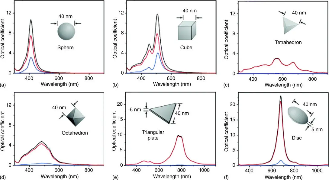
Figure 2.4 Calculated UV–visible extinction (black), absorption (red), and scattering spectra (blue) of Ag nanocrystals, illustrating the effect of shape on its spectral characteristics, including isotropic sphere (a), anisotropic cubes (b), tetrahedra (c), and octahedra (d), triangular plate (e) and circular disc (f).
Source: Wiley et al. 2006 [51]. Reproduced with permission of American Chemical Society.
(See online version for color figure).
For a faceted semiconductor, the surface electric field is a disparate situation. Besides the variation of the bandgap, the band edge position shifts as a function of different facets due to surface band bending. The different band edge positions provide varying redox potentials of the photogenerated electrons and holes, resulting in spatial separation of charge carriers and the built‐in electric field. In addition, selectively depositing a noble metal as cocatalysts on the surface facets can further enhance the strength of the built‐in electric field. When a single BiVO 4crystal enclosed by {010} and {011} facets was characterized by spatially resolved surface photovoltage spectroscopy (SRSPS), {011} facets exhibited a much higher signal intensity of surface photovoltage than {010} facet [52]. This phenomenon indicated a significant difference in surface band bending between BiVO 4{011} and {010} facets. As a consequence, the different band bending will lead to the variation in the spatial distribution of the charge carriers and build an electric field between different facets. By changing the area ratio of (011)/(010) facets of BiVO 4crystal, the surface built‐in electric field varied as well. Such an intrinsic difference in the surface photovoltage between different facets can be further enhanced by selectively depositing cocatalysts, such as MnO xand Pt deposited on faceted BiVO 4crystal, as shown in Figure 2.5[53].
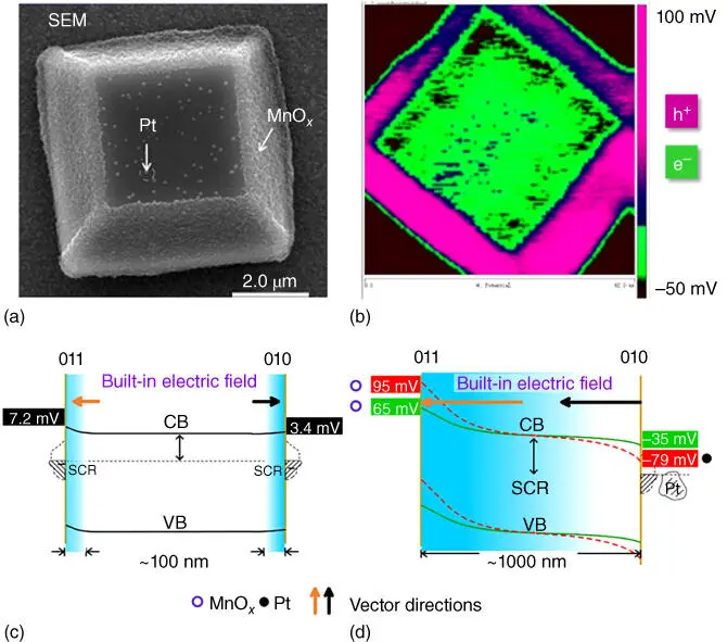
Figure 2.5 (a) Scanning electron microscopy (SEM) image of a BiVO 4single crystal with Pt photodeposited on {010} facet and MnO xphotodeposited on {011} facet. (b) Spatial distribution of the surface photovoltage signals. Pink and green colors correspond to holes and electrons separated toward the external surface, respectively. Schematic band diagrams across the border between the {011} and {010} facets of (c) a bare single BiVO 4photocatalyst particle and of (d) a single BiVO 4photocatalyst particle with MnO xcocatalyst selectively deposited at {011} facets (green line) and with MnO xand Pt nanoparticles selectively deposited at {011} and {010} facets, respectively (dashed pink line).
Source: Zhu et al. 2017 [53]. Reproduced with permission of American Chemical Society. (See online version for color figure.)
2.4 Effects of Facets Engineering
Each facet in a single crystal has different properties. However, combining anisotropic surface properties could dramatically alter the properties of the crystal, especially when the particle size is reduced to the nanoscale and the ratio of surface atoms/bulk atoms is no longer negligible.
2.4.1 Optical Properties
As mentioned previously, the surface electric field of a metal oscillates when the light strikes the surface. The oscillating electric field causes a rippling wave pattern in the spatial distribution of electrons. According to Lenz's law, the wave created by the surface plasmon opposes the electromagnetic wave of the incident light. The oscillating electrons absorb the energy of light and reemit the energy as the reflected light, due to which metals have shiny and reflective surfaces. However, when the particle size becomes very small, the surface plasmon is confined to a very small surface (i.e. LSPR). When the electron cloud is excited at one of the resonance frequencies, light absorption will become stronger. This is how LSPR frequency affects the light absorption of metal nanoparticles. The plasmon frequency is determined by electron density, dielectric constant, and effective mass of an electron. The well‐defined facets of a crystal form different shapes with more symmetries compared with spherical particles [54]. The surface charges tend to accumulate at edges and corners, which further promote surface polarization, i.e. the charge separation between mobile electrons and immobile atoms. Surface polarization determines the frequency and intensity of LSPR as it provides the main restoring force for electron oscillation. Large surface polarization reduces the restoring force, resulting in a redshift of resonance peak, and multiple distinct symmetries may induce several light absorption peaks [55]. Therefore, the same metal nanoparticles with different size and shape may exhibit different colors, indicating diverse light absorption.
Читать дальшеИнтервал:
Закладка:
Похожие книги на «Heterogeneous Catalysts»
Представляем Вашему вниманию похожие книги на «Heterogeneous Catalysts» списком для выбора. Мы отобрали схожую по названию и смыслу литературу в надежде предоставить читателям больше вариантов отыскать новые, интересные, ещё непрочитанные произведения.

Обсуждение, отзывы о книге «Heterogeneous Catalysts» и просто собственные мнения читателей. Оставьте ваши комментарии, напишите, что Вы думаете о произведении, его смысле или главных героях. Укажите что конкретно понравилось, а что нет, и почему Вы так считаете.