Electrical and Electronic Devices, Circuits, and Materials
Здесь есть возможность читать онлайн «Electrical and Electronic Devices, Circuits, and Materials» — ознакомительный отрывок электронной книги совершенно бесплатно, а после прочтения отрывка купить полную версию. В некоторых случаях можно слушать аудио, скачать через торрент в формате fb2 и присутствует краткое содержание. Жанр: unrecognised, на английском языке. Описание произведения, (предисловие) а так же отзывы посетителей доступны на портале библиотеки ЛибКат.
- Название:Electrical and Electronic Devices, Circuits, and Materials
- Автор:
- Жанр:
- Год:неизвестен
- ISBN:нет данных
- Рейтинг книги:3 / 5. Голосов: 1
-
Избранное:Добавить в избранное
- Отзывы:
-
Ваша оценка:
Electrical and Electronic Devices, Circuits, and Materials: краткое содержание, описание и аннотация
Предлагаем к чтению аннотацию, описание, краткое содержание или предисловие (зависит от того, что написал сам автор книги «Electrical and Electronic Devices, Circuits, and Materials»). Если вы не нашли необходимую информацию о книге — напишите в комментариях, мы постараемся отыскать её.
This outstanding new volume presents the basic concepts and fundamentals behind devices, circuits, and systems. It is a valuable reference for the veteran engineer and a learning tool for the student, the practicing engineer, or an engineer from another field crossing over into electrical engineering. It is a must-have for any library.
Electrical and Electronic Devices, Circuits, and Materials — читать онлайн ознакомительный отрывок
Ниже представлен текст книги, разбитый по страницам. Система сохранения места последней прочитанной страницы, позволяет с удобством читать онлайн бесплатно книгу «Electrical and Electronic Devices, Circuits, and Materials», без необходимости каждый раз заново искать на чём Вы остановились. Поставьте закладку, и сможете в любой момент перейти на страницу, на которой закончили чтение.
Интервал:
Закладка:
Where 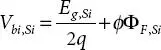 and
and 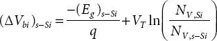
The induced channel strain (both uni-axial and bi-axial) modulates the threshold voltage of a MOSFET also. In [14], the strain induced threshold voltage shift is given by,
(1.20) 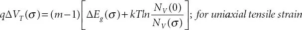
and
(1.21) 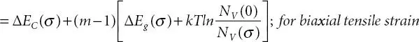
On the other hand, the impact of induced strain on the 2-D nature of electron in the inversion layer has been studied in [18] using Monte-Carlo simulation. For the behavior of holes in inversion layer of p-type strained silicon MOSFET, Michielis et al . [19] have proposed a new semi-analytical model and by using the new model, effective hole mobility has been calculated and validated with experimental data. Furthermore, Batwani et al . [20] have modeled the drain current under the influence of strain in the channel of a Si MOSFET and the expression of drift and diffusion component of output current are given by;
(1.22) 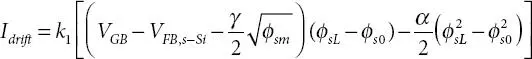
and
(1.23) 
The strain engineering is explored by the researchers in modern FET structures also. Chatterjee et al . [21] have modeled the carrier transport in partially embedded strained channel of a Nanowire-Field Effect Transistor (NW-FET) and found that under tensile strain, the phonon scattering occurs at the cost of electron energy, though when compressive strain is applied, then the electron gains energy during such scattering.
Thus, strain engineering is studied theoretically by several scientists for the last few decades and its impact is still under investigation for different new materials and device structures.
1.3 Simulation Studies in Strain Technology
Although several researchers are investigating the impact of strain on different aspects of material science and device performance theoretically, before using this technique in fabrication, various fabrication and device parameters need to be checked to keep the fabrication cost and time under control and predicting the results properly. In this regard, various Technology Computer Aided Design (TCAD) simulation software is designed by various companies, like Synopsys, Silvaco, Crosslight, Nano TCAD ViDES etc., and are currently being used by both academic researchers and the fabrication industry. These software use several mathematical- and physics-based models to estimate the impact of any changes on material and device properties and accordingly predict the device performance. As an example, the introduction of stress modifies the lattice constants and consequently, effective mass, mobility of the carrier changes significantly. Furthermore, induced stress modifies the band structure of semiconductor materials also. Due to these variations of material, several other depending parameters (e.g., conductivity, sensitivity, etc.) also vary and device performance parameters alter. The simulation software calculates the changed parameters of materials and device structure by using the mathematical and physical relationships among them. The researchers calibrate the simulator by validating the simulation data with the available experimental data to eliminate the errors, and then perform the required study in a virtual world. Thus, the simulators help to reduce the time of experiment, manufacturing cost and perform several studies with clear indicative results. In this section, several published simulation results will be discussed for better visual understanding of strain technology.
Since the invention of the modern Field Effect Transistor by J. E. Lilienfeld [1], researchers have been exploring different techniques to improve its performance further. Strain technology is one such technique where the transistor performance can be improved significantly without increasing the fabrication cost and time. The author has studied the impact of strain on the performance of uniaxially strain channel planner MOSFET device by using both Process and Device TCAD simulators of Synopsys and has found that the introduction of strain not only increases the device drive current, but also device transconductance and threshold voltage have improved significantly [22]. The virtual device structure and results of the studies are presented in Figure 1.1.
When the impact of biaxial stress on threshold voltage is studied, it has been found that channel doping modulation is required for such threshold voltage improvement, and as a result, half of the strain induced mobility improvement was lost [23]. After careful analysis of biaxial and uniaxial channel stress in MOSFET devices, scientists have found that uniaxial process-induced stress offers more benefits, in terms of fabrication cost and time, ease of implementation with standard CMOS fabrication process flow, etc., when compared with the substrate induced biaxial stress [4, 13, 23].
The advantages of uniaxial channel stress have been investigated in modern Fin channel Field Effect Transistors (FinFETs) by Xu et al . [24], and they have studied the impact of process-induced stress on the performance of aggressively scaled FinFET structure. The studies show that strain technology improves the modern transistor performance also and the work provides guidelines for optimizing FinFET stressor technology and performance enhancement trends for future technology nodes.
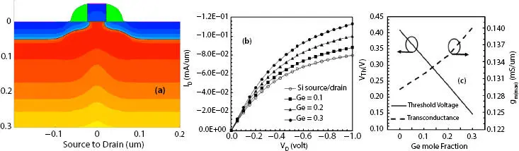
Figure 1.1 (a) The virtually fabricated p-MOSFET device structure (b) The output characteristics (I D- V D) of the transistor under study and (c) The variation of transconductance and threshold voltage of the p-MOSFET under study for different stressor material compositions [22].
The improvement of FinFET drive current due to induced strain, is thoroughly studied by Yu et al . [25]. The authors have performed full 3D process, stress, and device level simulation to quantify the impact of stress on device performance. The data shows good agreement with experimental data and it shows that channel mobility is higher, when compared with planner unstrained MOSFET device, due to lower transverse electric field. Furthermore, the stress engineering in cutting-edge 7-nm technology node transistor devices are also explored by Suyog Gupta et al . [26] using detailed simulation studies. They have investigated Group-IV materials (Si, Ge, Sn and their alloys) as stressor material in the source-drain regions of the transistor and proposed a new FinFET based CMOS design. Their investigations provide a path to sustain the technological scaling with improved device performance.
The effect of volume of the stressor material in the source-drain regions plays an important role to induce the channel stress. The present author has modulated the volume of stressor material (Si 1-xGe x) in Si as well as Ge FinFET device structures and the results are analyzed thoroughly [27, 28]. The study revealed that by changing the volume of SiGe material, in the fractionally filled embedded source-drain regions, the channel stress could be altered between tensile and compressive stress. The tensile channel stress is required to improve the performance of n- channel FET, and channel stress should be compressive in nature to improve p- channel FET performance [29]. In these works, for the first time a new technique has been proposed where without increasing any fabrication cost, the p- and n- channel FinFET performance improves by using strain technology in a suitable manner. The simulated device structure and channel stress variation for various SiGe length from channel interface inside source-drain regions of the study [27] are shown in Figure 1.2.
Читать дальшеИнтервал:
Закладка:
Похожие книги на «Electrical and Electronic Devices, Circuits, and Materials»
Представляем Вашему вниманию похожие книги на «Electrical and Electronic Devices, Circuits, and Materials» списком для выбора. Мы отобрали схожую по названию и смыслу литературу в надежде предоставить читателям больше вариантов отыскать новые, интересные, ещё непрочитанные произведения.


Обсуждение, отзывы о книге «Electrical and Electronic Devices, Circuits, and Materials» и просто собственные мнения читателей. Оставьте ваши комментарии, напишите, что Вы думаете о произведении, его смысле или главных героях. Укажите что конкретно понравилось, а что нет, и почему Вы так считаете.