Electrical and Electronic Devices, Circuits, and Materials
Здесь есть возможность читать онлайн «Electrical and Electronic Devices, Circuits, and Materials» — ознакомительный отрывок электронной книги совершенно бесплатно, а после прочтения отрывка купить полную версию. В некоторых случаях можно слушать аудио, скачать через торрент в формате fb2 и присутствует краткое содержание. Жанр: unrecognised, на английском языке. Описание произведения, (предисловие) а так же отзывы посетителей доступны на портале библиотеки ЛибКат.
- Название:Electrical and Electronic Devices, Circuits, and Materials
- Автор:
- Жанр:
- Год:неизвестен
- ISBN:нет данных
- Рейтинг книги:3 / 5. Голосов: 1
-
Избранное:Добавить в избранное
- Отзывы:
-
Ваша оценка:
Electrical and Electronic Devices, Circuits, and Materials: краткое содержание, описание и аннотация
Предлагаем к чтению аннотацию, описание, краткое содержание или предисловие (зависит от того, что написал сам автор книги «Electrical and Electronic Devices, Circuits, and Materials»). Если вы не нашли необходимую информацию о книге — напишите в комментариях, мы постараемся отыскать её.
This outstanding new volume presents the basic concepts and fundamentals behind devices, circuits, and systems. It is a valuable reference for the veteran engineer and a learning tool for the student, the practicing engineer, or an engineer from another field crossing over into electrical engineering. It is a must-have for any library.
Electrical and Electronic Devices, Circuits, and Materials — читать онлайн ознакомительный отрывок
Ниже представлен текст книги, разбитый по страницам. Система сохранения места последней прочитанной страницы, позволяет с удобством читать онлайн бесплатно книгу «Electrical and Electronic Devices, Circuits, and Materials», без необходимости каждый раз заново искать на чём Вы остановились. Поставьте закладку, и сможете в любой момент перейти на страницу, на которой закончили чтение.
Интервал:
Закладка:
Since the strain tensor is symmetrical in nature, the strain tensor can be diagonalized by appropriate coordinate transformation. After diagonalizing the strain tensor in a system, the modified distance Δ L ′ can be expressed as,
(1.5) 
So, for a small displacement along an axis α = ξ, ν, ζ, the change in length (L α) becomes,
(1.6) 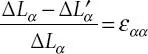
The strain tensor in this case simplified to,
(1.7) 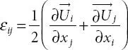
The strain tensor, in general, can be written in terms of individual strain co-efficient (ε αβ), and is given by [4],
(1.8) 
The stress components for any lattice surface can be obtained from equation ( 1.8).
1.2.2 Stress Matrix for Biaxial and Uniaxial Stress
Now the uniaxial stress is defined as induced stress directed predominantly along any one axis. On the other hand, for biaxial stress, the induced stress is directed along two perpendicular axis direction. For [001] and [110] surface, the uniaxial stress after simplification of (1.8) becomes [4],
(1.9) 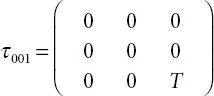
(1.10) 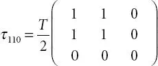
Since from Hooke’s law it can be written that stress is proportional to strain, therefore,
(1.11) 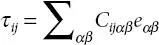
Where C ijαβare called elastic stiffness constant. As stress and strain tensors are both symmetrical in nature, so these can be written in terms of a six component array and the elastic stiffness tensor reduces to a 6×6 matrix
(1.12) 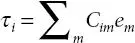
In case of cubic crystal structure, the stiffness constant matrix in equation ( 1.12) becomes a simple form as [4],
(1.13) 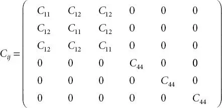
Introduction of strain technology to improve material parameters was theoretically published by several researchers in the 1950s [5–7]; however, this technology was implemented in transistor fabrication started only in the 1980s [8, 9]. The initial works of stress incorporation in the channel of a MOSFET structure was performed by using a SiGe virtual substrate and on top of that a thin Si layer was deposited as channel region [10]. The lattice mismatch at the interface of virtual substrate and thin channel layer creates a biaxial stress in the Si channel which reduces both the inter-valley scattering and effective mass of the carriers. As a result, the conductivity of carriers through the channel increases and transistor performance improves. When a thin semiconductor layer is grown on top of a <001> semiconductor surface, then the induced biaxial stress has been theoretically expressed by several researchers and the strain tensor in this case becomes [4];
(1.14) 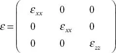
However, the challenges with biaxial channel stress is that it creates traps and defects along the channel, performance loss at high vertical field along with the degradation of Si-SiGe interface quality due to out-diffusion of Ge from the virtual substrate region [11].
To overcome these challenges of biaxial stress, a new technique of channel stress incorporation was introduced where instead of using SiGe virtual substrate, the source and drain regions are embedded with SiGe material, such that stress is induced in the channel from the interfaces of source-channel and drain-channel interfaces [12]. The advantage of this new technique is that the induced stress in the channel is uniaxial, and it improves both hole and electron mobility in the high vertical field when compared with biaxial strained channel. In addition, the induced uniaxial stress also improves the drive current significantly in nano-scale MOSFETs [13]. Therefore, in the case of uniaxial channel stress, the lattice mismatch at channel-source/drain interfaces creates an induced stress towards the channel from the interfaces, which is directed predominantly in one direction, and for this induced stress, the uniaxial strain tensor takes the following form [4]:
(1.15) 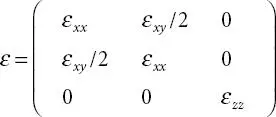
1.2.3 Impact of Strain on MOSFET Parameters
The effect of strain-induced changes on semiconductor properties and CMOS device performances have long been studied extensively by researchers. Lim et al . [14] and Numata et al . [15] has modeled the impact of strain on the strained-Si band structure as:
(1.16) 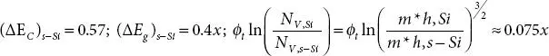
Where x is the Ge mole fraction in Si (1-x)Ge xsubstrate. Furthermore, in [15] and [16], the energy band parameters are also calculated for strained Si material and is given by,
(1.17) 
Where (∆E g) SiGeis the reduced band gap of SiGe from Si. Zhang and Fossum [17] have calculated the flat band voltage and built-in voltage across channel-source and drain-channel interface in MOSFETs where strained-Si have been used as channel material, and the flat band voltage is given by,
(1.18) 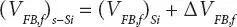
Where, 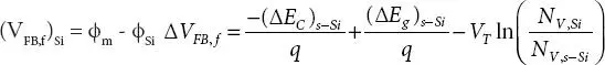 and, the built in voltage is given by,
(1.19) 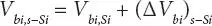
Интервал:
Закладка:
Похожие книги на «Electrical and Electronic Devices, Circuits, and Materials»
Представляем Вашему вниманию похожие книги на «Electrical and Electronic Devices, Circuits, and Materials» списком для выбора. Мы отобрали схожую по названию и смыслу литературу в надежде предоставить читателям больше вариантов отыскать новые, интересные, ещё непрочитанные произведения.


Обсуждение, отзывы о книге «Electrical and Electronic Devices, Circuits, and Materials» и просто собственные мнения читателей. Оставьте ваши комментарии, напишите, что Вы думаете о произведении, его смысле или главных героях. Укажите что конкретно понравилось, а что нет, и почему Вы так считаете.