Electrical and Electronic Devices, Circuits, and Materials
Здесь есть возможность читать онлайн «Electrical and Electronic Devices, Circuits, and Materials» — ознакомительный отрывок электронной книги совершенно бесплатно, а после прочтения отрывка купить полную версию. В некоторых случаях можно слушать аудио, скачать через торрент в формате fb2 и присутствует краткое содержание. Жанр: unrecognised, на английском языке. Описание произведения, (предисловие) а так же отзывы посетителей доступны на портале библиотеки ЛибКат.
- Название:Electrical and Electronic Devices, Circuits, and Materials
- Автор:
- Жанр:
- Год:неизвестен
- ISBN:нет данных
- Рейтинг книги:3 / 5. Голосов: 1
-
Избранное:Добавить в избранное
- Отзывы:
-
Ваша оценка:
Electrical and Electronic Devices, Circuits, and Materials: краткое содержание, описание и аннотация
Предлагаем к чтению аннотацию, описание, краткое содержание или предисловие (зависит от того, что написал сам автор книги «Electrical and Electronic Devices, Circuits, and Materials»). Если вы не нашли необходимую информацию о книге — напишите в комментариях, мы постараемся отыскать её.
This outstanding new volume presents the basic concepts and fundamentals behind devices, circuits, and systems. It is a valuable reference for the veteran engineer and a learning tool for the student, the practicing engineer, or an engineer from another field crossing over into electrical engineering. It is a must-have for any library.
Electrical and Electronic Devices, Circuits, and Materials — читать онлайн ознакомительный отрывок
Ниже представлен текст книги, разбитый по страницам. Система сохранения места последней прочитанной страницы, позволяет с удобством читать онлайн бесплатно книгу «Electrical and Electronic Devices, Circuits, and Materials», без необходимости каждый раз заново искать на чём Вы остановились. Поставьте закладку, и сможете в любой момент перейти на страницу, на которой закончили чтение.
Интервал:
Закладка:
Abstract
Generation of thermal strain while fabricating modern nano-scale Metal-Oxide-Semiconductor-Field-Effect-Transistor (MOSFET) devices is inevitable since the standard CMOS fabrication process includes various high and low thermal stages. Different regions and materials of a MOSFET behave differently due to their difference in thermal expansion co-efficient and it leads to the generation of thermal stress within the device. Various researchers have studied the impact of strain on material and device characteristics in the last few decades through theoretical calculations, software simulations and various experiments and found that introduction of controlled strain within the transistor active region can be used to improve device performance. In this chapter, various theoretical, simulation and experimental research works on strain engineering are discussed in brief. Gradual development of this performance-enhancing technique is also included along with some of the latest reports in this field of research in modern devices.
Keywords:Strain, stress, MOSFET, FinFET, silicon-germanium (SiGe)
1.1 Introduction
The last century has witnessed the growth of physics and technology to a new height. In 1930, J. E. Lilienfield invented and filed a patent [1] for a new device structure called MOSFET that later became an integral part of modern technology. In addition, in the field of material science, the innovation of silicon (Si) as semiconductor material opened a new field of research where the conductivity of a material can be varied according to the requirement. Particularly from the late 1940s, several researchers started publishing various theoretical research findings in this new domain of physics. From the early 1960s, the fabrication of MOSFET started, and technological development has grown very rapidly since then.
In 1965, Gordon Moore proposed his famous prediction on future technological progress that the number of transistors in an Integrated Circuit (IC) will double in every 18 months [2] and this law was followed by the industry for a long time by gradually reducing the dimensions of the transistor. However, as the physics of planner Si MOSFET operation started approaching its fundamental limit in reduced dimensions, scientists started looking for alternatives to dimensional reductions to sustain the technological growth. In this regard, several new semiconductor materials (e.g., GaAs, InGaAs, Graphene, MoS 2etc.) are studied in place of Si to identify the possible alternative to it. In addition, various new device structures of transistor are also explored to overcome the challenges of MOSFET in such small-scaled dimensions. Among the new transistor structures, the FinFET device has been accepted by both academia and industry due to its several advantages over the other devices. Currently the latest processors are designed by leading companies by using FinFET devices to perform the high-speed operations with improved performance.
On the other hand, there are many scientists working on the performance improvement techniques such that the improved performance of lower dimensional structures can be achieved at higher dimensional devices and the challenges of lower dimensions can be avoided. Among these performance enhancement techniques, strain engineering has been emerging as the most feasible approach, and leading companies are using this technique currently to improve the performance of their transistors. However, there are many unknown areas in strain technology, and it needs to be explored further so that it can be used in new devices also.
In this chapter, gradual discoveries of strain engineering are discussed in brief for better understanding of how this performance enhancement technique has developed. In Section 1.2, theoretical analysis of strain engineering by various researchers is discussed. Strain affects various properties of material, like the band structure, conductivity, carrier mobility, etc., and how strain-induced changes modify the device parameters are calculated by several researchers and published in reputed journals and conferences. Some of these results are discussed in brief. In Section 1.3, different simulation studies on strain engineering are included. Various simulation data are compared with theoretical and experimental data to validate the simulation results, and future technological data are predicted by using the calibrated simulators. These simulations help to forecast the output of any new device or technique which is yet to be fabricated or implemented, and in this way the simulation process helps to continue future research without worrying about the fabrication cost and time. Due to these reasons, both scientists and fabrication companies are now depending upon the data shown by properly calibrated simulation software. In Section 1.4, various experimental results on strain engineering are shown and compared with theoretical and simulated data. In the last few decades, various scientists have explored strain engineered FET devices through several experiments and these results indicate that by using this performance enhancement technique, several challenges of unstrained nano-scale transistors can be overcome. Although there are not many laboratories to fabricate these modern FETs, many published reports are available to validate the theoretically and simulated predictions in this field of strain engineering. Some of these experimental data are discussed in brief to get some idea on real-time fabrication output. Finally, in Section 1.5, a summary of this chapter is discussed in brief and some possible future research problems in this area are included.
1.2 Theory of Strain Technology
1.2.1 Stress and Strain
Strain: The result of applying force which slightly deform/misalign the atomic structure of a material.
Stress: It is the result of strain in any material.
Therefore, it can be said that by applying some external force, if the atomic arrangements of a material can be altered slightly, then interatomic force will change, and as a result, the material will be called stressed/strained material.
Now, let us consider a point P having radius vector rand position vector (x, y, z) under stable condition. When an external force is applied, the point P shifted slightly at P’ and the new radius vector becomes r’and new position vector becomes (x’, y’, z’). The displacement is given by [3];
(1.1) 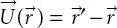
and this displacement gives the measure of deformation of the material under strain quantitatively. The distance between the two points can be found by using the following relation:
(1.2) 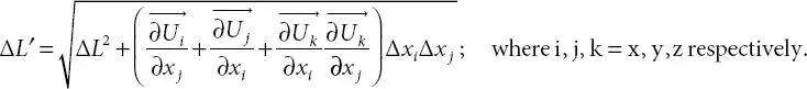
 is the distance in the relaxed solid.
Using the strain tensor matrix, equation ( 1.2) can be further written as,
(1.3) 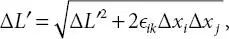
(1.4) 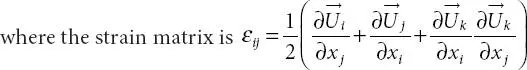
Интервал:
Закладка:
Похожие книги на «Electrical and Electronic Devices, Circuits, and Materials»
Представляем Вашему вниманию похожие книги на «Electrical and Electronic Devices, Circuits, and Materials» списком для выбора. Мы отобрали схожую по названию и смыслу литературу в надежде предоставить читателям больше вариантов отыскать новые, интересные, ещё непрочитанные произведения.


Обсуждение, отзывы о книге «Electrical and Electronic Devices, Circuits, and Materials» и просто собственные мнения читателей. Оставьте ваши комментарии, напишите, что Вы думаете о произведении, его смысле или главных героях. Укажите что конкретно понравилось, а что нет, и почему Вы так считаете.