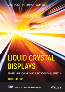
Ernst Lueder - Liquid Crystal Displays
Здесь есть возможность читать онлайн «Ernst Lueder - Liquid Crystal Displays» — ознакомительный отрывок электронной книги совершенно бесплатно, а после прочтения отрывка купить полную версию. В некоторых случаях можно слушать аудио, скачать через торрент в формате fb2 и присутствует краткое содержание. Жанр: unrecognised, на английском языке. Описание произведения, (предисловие) а так же отзывы посетителей доступны на портале библиотеки ЛибКат.
- Название:Liquid Crystal Displays
- Автор:
- Жанр:
- Год:неизвестен
- ISBN:нет данных
- Рейтинг книги:4 / 5. Голосов: 1
-
Избранное:Добавить в избранное
- Отзывы:
-
Ваша оценка:
- 80
- 1
- 2
- 3
- 4
- 5
Liquid Crystal Displays: краткое содержание, описание и аннотация
Предлагаем к чтению аннотацию, описание, краткое содержание или предисловие (зависит от того, что написал сам автор книги «Liquid Crystal Displays»). Если вы не нашли необходимую информацию о книге — напишите в комментариях, мы постараемся отыскать её.
THE NEW EDITION OF THE GOLD-STANDARD IN TEACHING AND REFERENCING THE FUNDAMENTALS OF LCD TECHNOLOGIES
Liquid Crystal Displays — читать онлайн ознакомительный отрывок
Ниже представлен текст книги, разбитый по страницам. Система сохранения места последней прочитанной страницы, позволяет с удобством читать онлайн бесплатно книгу «Liquid Crystal Displays», без необходимости каждый раз заново искать на чём Вы остановились. Поставьте закладку, и сможете в любой момент перейти на страницу, на которой закончили чтение.
Интервал:
Закладка:
19 Chapter 20Figure 20.1 Single light valve colour projectorFigure 20.2 A single light valve field sequential colour projectorFigure 20.3 Single light valve scrolling projectorFigure 20.4 Generation of scrolling colour bands by a rotating prismFigure 20.5 Single light valve angular colour separation projectionFigure 20.6 A single light valve projector with colour gratingFigure 20.7 Three light valve projector with three equal optic pathsFigure 20.8 Three light valve projector with unequal optic pathsFigure 20.9 Projector with three reflective LC light valvesFigure 20.10 A projector with three LCOS light valvesFigure 20.11 Projector with two light valvesFigure 20.12 A rear projector with one or three light valvesFigure 20.13 A projector with three optically addressed LC light valves
20 Chapter 21Figure 21.1 Explanation of the shadow figure in reflective displaysFigure 21.2 Distortion of a rectangular isotropic bodyFigure 21.3 The expansion of a PES substrate versus d land d sfor α s= 44 ppm/K, α l= 5 ppm/K E s= 2.6 kN/mm 2(PES) and E t= 86 kN/mm 2in Equation (21.3) (Grimsdilch et al ., 1978); (b) the tangential tension σ versus d land d sfor the same parameters as in Figure 21.3(a); (c) diagonal L Dof a square versus Δ T for a constant distortion in μm as parametersFigure 21.4 Input characteristics of a-Si :H TFTs fabricated at different process temperaturesFigure 21.5 Variation of V thduring BT stress of a-Si :H TFTs fabricated at various temperaturesFigure 21.6 Input characteristics of poly-Si TFTs fabricated at 250 °C and 200 °CFigure 21.7 Transfer steps of an LCD fabricated at high temperature to a flexible substrate (SUFLA). This figure was reproduced from Miyasaka, M., SID 07 , p. 1673 with permission by The Society for Information DisplayFigure 21.8 SUFLA transfer yield versus display area. This figure was reproduced from Miyasaka, M., SID 07 , p. 1675 with permission by The Society for Information DisplayFigure 21.9 I D– V Gcharacteristics of an a-Si TFT on a thinned stainless steel substrate after 250 °C processing, heat treatment and a bias temperature stress (BTS). This figure was reproduced from Kim, C. D. et al. , SID 09 , p. 195 with permission by The Society for Information Display
21 Chapter 22Figure 22.1 Flexographic printingFigure 22.2 Knife coatingFigure 22.3 Ink-jet printing systemFigure 22.4 Printing head with piezo-electric elementFigure 22.5 Maximum radius versus speed of droplet with surface tension γλ as parameterFigure 22.6 Ultrasonic ink-jet printer. This figure was reproduced from Amemiya, I. et al., SID 07 , p. 1603 with permission by The Society for Information DisplayFigure 22.7 Profile of droplet in an ultrasonic ink-jet printer. This figure was reproduced from Amemiya, I. et al., SID 07 , p. 1604 with permission by The Society for Information DisplayFigure 22.8 Silk screen printingFigure 22.9 Wetting angle α of a liquidFigure 22.10 Process chamber of plasma cleaningFigure 22.11 UV–ozone cleaning chamberFigure 22.12 Free surface energy γ sof ITO versus duration of UV–ozone cleaningFigure 22.13 Change of free surface energy of ITO during storage time. This figure was reproduced from Souk, J. H. et al., SID 08 , p. 431 with permission by The Society for Information DisplayFigure 22.14 The ink-jet print bounded by a wall of a black matrix (a) before and (b) after baking. This figure was reproduced from Liu, K. H. et al., SID 07 , p. 1607 with permission by The Society for Information DisplayFigure 22.15 Interlaced ink-jet heads for uniform printing on a larger areaFigure 22.16 Transmittance–voltage curve of a vacuum filled and of a flexographically printed nematic LC. This figure was reproduced from Kawashima, N. et al., SID 09 , p. 25 with permission by The Society for Information DisplayFigure 22.17 Cross-section of an OTFT with a small molecule organic semiconductor. This figure was reproduced from Kawashima, N. et al., SID 09 , p. 26 with permission by The Society for Information DisplayFigure 22.18 I d– V Gcharacteristic of the OTFT in Figure 22.16. This figure was reproduced from Yase, K. et al ., SID 09 , p. 199 with permission by The Society for Information DisplayFigure 22.19 Two-step micro contact printing for OTFTs. This figure was reproduced from Yase, K. et al., SID 09 , p. 199 with permission by The Society for Information DisplayFigure 22.20 Cross-section of an OTFT with a polymer based organic semiconductor. This figure was reproduced from Yase, K. et al., SID 09 , p. 200 with permission by The Society for Information DisplayFigure 22.21 I d– V Gcharacteristics of the OTFT in Figure 22.19Figure 22.22 Cell building by lamination of plastic substrates
22 Chapter 23Figure 23.1 (a) Cross-sectional transmission electron microscope surface of crystalline IGZO; (b) diagram of the crystalline layers. This figure was reproduced from Matsuo, T. et al . (2014), SID Symp. Digest Tech. Papers 45 , pp. 83–86 with permission by The Society for Information DisplayFigure 23.2 Band gap diagram of c -axis aligned IGZO (CAAC-IGZO). This figure was reproduced from Yamazaki and Tsutsui (2017), p.96, fig 2.87, with permission by John Wiley and Sons Inc.Figure 23.3 Drain current ( I D)–gate voltage ( V G) input of a-Si, oxide semiconductors and LT PS. This figure was reproduced from Matsuo, T. et al . (2014), SID Symp. Digest Tech. Papers 45 , pp. 83–86 with permission by The Society for Information DisplayFigure 23.4 Transmittance of an IGZO layer. This figure was reproduced from Yamashita, A. et al . (2015), JSID , 22, pp. 216–227 with permission by The Society for Information Display.Figure 23.5 Crystalline (a, c) and amorphous (b, d) atomic structures of IGZO. This figure was reproduced from Kamiya, T., et al . (2013), SID 44 , pp. 11–13 with permission by The Society for Information DisplayFigure 23.6 Saturation and linear mobility in an oxide TFTFigure 23.7 Progress flow and structure of bottom-gate, bottom-contact TFT. This figure was reproduced from Osada, T., et al . (2009), SID 40 , pp. 184–187 with permission by The Society for Information DisplayFigure 23.8 I D– V Gcurve of an amorphous In-Ga-Zn-oxide TFT. This figure was reproduced from Osada, T., et al . (2009), SID 40 , pp. 184–187 with permission by The Society for Information DisplayFigure 23.9 Bottom-gate etch-stop transistor. This figure was reproduced from Yamazaki and Tsutsui (2017), p.5, fig 2.3a, with permission by John Wiley and Sons Inc.Figure 23.10 Schematic diagram of a three-layer structure of ITZO-TFTs. This figure was reproduced from Tsai M., et al . (2015), SID 46 , with permission by The Society for Information DisplayFigure 23.11 (a, b) I D= f ( V G) and mobility and sub-threshold voltage swing ( SS ) for a single-layer IGZO-TFT (a) and a single-layer ITZO-TFT (b). This figure was reproduced from Tsai M., et al . (2015), SID 46 , with permission by The Society for Information DisplayFigure 23.12 I D= f ( V G) and mobilities and SS values for the two single layers and the triple layer, the triple-layer device working in enhancement mode. This figure was reproduced from Tsai M., et al . (2015), SID 46 , with permission by The Society for Information DisplayFigure 23.13 View of a display with split source, drain and semiconductor electrodes and cross-section of bottom-gate etch-stop TFT. This figure was reproduced from Lee, S. et al . (2018) JSID , 26, pp. 164–168 with permission by The Society for Information DisplayFigure 23.14 (a, b) I D= f ( V G) for a conventional and a split TFT (a) and field effect mobility for a conventional and a split TFT (b). This figure was reproduced from Lee, S. et al . (2018) JSID , 26, pp. 164–168 with permission by The Society for Information DisplayFigure 23.15 (a, b) PBTS for I D= f ( V G) for a conventional (a) and a split (b) electrode TFT with stress times of up to 3.6 ks. This figure was reproduced from Lee, S. et al . (2018) JSID , 26, pp. 164–168 with permission by The Society for Information DisplayFigure 23.16 Cross-section of dual-gate back-channel etched IGZTO-TFT. This figure was reproduced from Nakata, M., et al . (2019) SID 50 : 1226–1229 with permission by The Society for Information DisplayFigure 23.17 The various categories of crystalline layers. This figure was reproduced from Yamashita, A. et al . (2015), SID Symp. Digest Tech. Papers 45 , pp. 263–266 with permission by The Society for Information DisplayFigure 23.18 Mobility as a function of atomic percent of N concentration. Lee, E. et al . (2015), SID , p. 681 266 with permission by The Society for Information DisplayFigure 23.19 Bottom-gate top conductor TFT with capacitor. This figure was reproduced from Yamazaki, S. (2014), SID, 45 , p. 9 with permission by The Society for Information DisplayFigure 23.20 Hall mobility of nIGZO and CAAC-IGZO. This figure was reproduced from Ishihara, N. et al . (2016), SID Symp. Digest Tech. Papers, 47 , p. 816 with permission by The Society for Information DisplayFigure 23.21 Cross-section of the layers of a printed TFT. S, semiconductor. This figure was reproduced from Chena, Y. et al . (2016), p. 322, SID Symp. Digest Tech. Papers, 47 with permission by The Society for Information DisplayFigure 23.22 I D= f ( V G) of an all-printed oxide TFT. This figure was reproduced from Matsumoto, S. et al . (2015), SID 46 , p. 300 with permission by The Society for Information DisplayFigure 23.23 (a, b) Structures for a printed TFT before (a) and after (b) irradiation for conductivity enhancement. This figure was reproduced from Bermundo, J. et al . (2019), SID 50 , pp. 422–425 with permission by The Society for Information DisplayFigure 23.24 I D= f ( V G) after UV and krypton fluoride (KrF) excimer laser irradiation of all-printed layers. This figure was reproduced from Bermundo, J. et al . (2019), SID 50 , pp. 422–425 with permission by The Society for Information DisplayFigure 23.25 (a, b) Layers of a single-gate TFT under tensile stress (a) and under compressive stress (b). This figure was reproduced from Billah, M. et al . (2016), SID 47 , p. 1155 with permission by The Society for Information DisplayFigure 23.26 (a, b) I D= f ( V G) for a single-gate TFT (a) and a dual-gate TFT (b) under tensile and compressive stress. This figure was reproduced from Billah, M. et al . (2016), SID 47 , p. 1155 with permission by The Society for Information DisplayFigure 23.27 I D= f ( V G) under NBIS for a single-gate (a) and a dual-gate TFT (b) and for bending stress for a single-gate (c) and a dual-gate TFT (d). This figure was reproduced from Billah, M.M. and Jang, J. (2019) SID 50 , pp. 210–213 with permission by The Society for Information DisplayFigure 23.28 A V thin for the time under NBIS (a) and under tensile strain (b) for single- and dual-gate driving and the mobility under NBIS (c) and tensile stress (d) for single- and dual-gate driving. This figure was reproduced from Billah, M.M. and Jang, J. (2019) SID 50 , pp. 210–213 with permission by The Society for Information DisplayFigure 23.29 Wavelength of the UWB-TFT and the a-IGZO-TFT. This figure was reproduced from Kim, J. et al . (2016), SID Symp. Digest Tech. Papers, 47 with permission by The Society for Information DisplayFigure 23.30 (a, b) NBIS stability under white LED illumination for the a-IGZO TFT (a) and the UWB-aOS TFT (b). This figure was reproduced from Kim, J. et al . (2016), SID Symp. Digest Tech. Papers, 47 with permission by The Society for Information DisplayFigure 23.31 (a, b) Stability under fluorescent lamp illumination for a-IGZO TFT (a) and UWB-aOS TFT (b). This figure was reproduced from Kim, J. et al . (2016), SID Symp. Digest Tech. Papers, 47 with permission by The Society for Information DisplayFigure 23.32 (a, b) PBTS test for a non-split (a) and a split-layer TFT (b). This figure was reproduced from Lee, S. et al . (2019) SID Symp. Digest Tech, Papers 50 , pp. 1263–1266 with permission by The Society for Information DisplayFigure 23.33 (a, b) Bending test for a non-split TFT (a) and a split-layer TFT (b). This figure was reproduced from Lee, S. et al . (2019) SID Symp. Digest Tech, Papers 50 , pp. 1263–1266 with permission by The Society for Information DisplayFigure 23.34 Cross-linking of styrene-based polymer (PC200) into a conductor. This figure was reproduced from Oku, S. (2018), SID 49 , pp. 794–796 with permission by The Society for Information DisplayFigure 23.35 Patterning of electrodes by PVPU irradiation. This figure was reproduced from Oku, S. (2018), SID 49 , pp. 794–796 with permission by The Society for Information DisplayFigure 23.36 Schematic illustration of the fabricated organic TFT. This figure was reproduced from Oku, S. (2018), SID 49 , pp. 794–796 with permission by The Society for Information DisplayFigure 23.37 I D= f ( V G) for the organic TFT. This figure was reproduced from Oku, S. (2018), SID 49 , pp. 794–796 with permission by The Society for Information DisplayFigure 23.38 Mobility of the organic TFT depending on the channel length. This figure was reproduced from Oku, S. (2018), SID 49 , pp. 794–796 with permission by The Society for Information DisplayFigure 23.39 I D= f ( V G) diagram of an OTFT with Al and Au electrodes. This figure was reproduced from Katsuhara, M. et al . (2014), Symp. Digest Tech. Papers, 45 , pp. 716–719 with permission by The Society for Information DisplayFigure 23.40 The mobilities μ obefore and μ Rafter bending test of an OTFT with radius R < 10 mm. This figure was reproduced from Katsuhara, M. et al . (2014), Symp. Digest Tech. Papers, 45 , pp. 716–719 with permission by The Society for Information DisplayFigure 23.41 The conventional five photolithographic steps for one pattern. This figure was reproduced from Kaelblein, D. et al . (2016), SID 47 , p. 869 with permission by The Society for Information DisplayFigure 23.42 Photolithography with direct patterning of an organic semiconductor in two steps. This figure was reproduced from Kaelblein, D. et al . (2016), SID 47 , p. 869 with permission by The Society for Information DisplayFigure 23.43 Transfer characteristics of 10 photopatterned organic transistors. This figure was reproduced from Kaelblein, D. et al . (2016), SID 47 , p. 869 with permission by The Society for Information DisplayFigure 23.44 I D= f ( V G) of an organic TFT with a mobility of 4 cm 2/Vs. This figure was reproduced from Kaelblein, D. et al . (2016), SID 47 , p. 869 with permission by The Society for Information DisplayFigure 23.45 The upper half of a liquid crystal cell with rotated molecules and vertical alignment.
Читать дальшеИнтервал:
Закладка:
Похожие книги на «Liquid Crystal Displays»
Представляем Вашему вниманию похожие книги на «Liquid Crystal Displays» списком для выбора. Мы отобрали схожую по названию и смыслу литературу в надежде предоставить читателям больше вариантов отыскать новые, интересные, ещё непрочитанные произведения.
Обсуждение, отзывы о книге «Liquid Crystal Displays» и просто собственные мнения читателей. Оставьте ваши комментарии, напишите, что Вы думаете о произведении, его смысле или главных героях. Укажите что конкретно понравилось, а что нет, и почему Вы так считаете.
