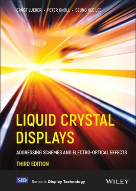
Ernst Lueder - Liquid Crystal Displays
Здесь есть возможность читать онлайн «Ernst Lueder - Liquid Crystal Displays» — ознакомительный отрывок электронной книги совершенно бесплатно, а после прочтения отрывка купить полную версию. В некоторых случаях можно слушать аудио, скачать через торрент в формате fb2 и присутствует краткое содержание. Жанр: unrecognised, на английском языке. Описание произведения, (предисловие) а так же отзывы посетителей доступны на портале библиотеки ЛибКат.
- Название:Liquid Crystal Displays
- Автор:
- Жанр:
- Год:неизвестен
- ISBN:нет данных
- Рейтинг книги:4 / 5. Голосов: 1
-
Избранное:Добавить в избранное
- Отзывы:
-
Ваша оценка:
- 80
- 1
- 2
- 3
- 4
- 5
Liquid Crystal Displays: краткое содержание, описание и аннотация
Предлагаем к чтению аннотацию, описание, краткое содержание или предисловие (зависит от того, что написал сам автор книги «Liquid Crystal Displays»). Если вы не нашли необходимую информацию о книге — напишите в комментариях, мы постараемся отыскать её.
THE NEW EDITION OF THE GOLD-STANDARD IN TEACHING AND REFERENCING THE FUNDAMENTALS OF LCD TECHNOLOGIES
Liquid Crystal Displays — читать онлайн ознакомительный отрывок
Ниже представлен текст книги, разбитый по страницам. Система сохранения места последней прочитанной страницы, позволяет с удобством читать онлайн бесплатно книгу «Liquid Crystal Displays», без необходимости каждый раз заново искать на чём Вы остановились. Поставьте закладку, и сможете в любой момент перейти на страницу, на которой закончили чтение.
Интервал:
Закладка:
14 Chapter 15Figure 15.1 Cross-section of a p -channel and n -channel poly-Si TFTFigure 15.2 Fabrication steps of a top-gate poly-Si TFTFigure 15.3 V thdependent on the dose of B doping in the channels of n -channel and p -channel poly-Si TFTs. Reproduced from Iberaki, 1999 with permission of John Wiley & Sons.Figure 15.4 Transfer characteristics of n - and p -channel poly-Si TFTs. Reproduced from Iberaki, 1999 with permission of John Wiley & Sons.Figure 15.5 Fabrication steps of a bottom-gate poly-Si TFTFigure 15.6 Grain with super lateral growth region dependent on the scanning laser doseFigure 15.7 Grain size with super lateral growth region dependent on large area laser doseFigure 15.8 REM photograph of grain size after four large area laser shotsFigure 15.9 The reflow method for generating LDD and n+ areas: (a) implantation before and (b) after reflow of photoresistFigure 15.10 Implantation with an anodized Ta mask (a) for contacts and (b) with Ta 2O 5etched off for LDDFigure 15.11 Oblique implantation for LDD and contacts simultaneouslyFigure 15.12 The Lateral Body Terminal (LBT) for the reduction of the kink currentFigure 15.13 The circuit concept for a 202 dpi display with poly-Si drivers on glass and further ICs on an external circuit boardFigure 15.14 The circuit concept of a high-resolution displayFigure 15.15 Circuit diagram of a 6-bit poly-Si data driverFigure 15.16 A 5-bit D/A converter with γ correction in poly-Si technology
15 Chapter 16Figure 16.1 Cross-section of LCOS addressing devicesFigure 16.2 Pixel FET Sand storage capacitor C Gof an LCOS arrayFigure 16.3 The time slots for a pixel with 5-bit grey shades. Numbers ν on top indicate weight 2 νof a bit; numbers s below indicate if SRAM number 1 or number 2 feeds in the informationFigure 16.4 Block parallel addressing with four blocks and the time slots for 5-bit grey shades in each blockFigure 16.5 Digital block addressing in which SRAM outputs are required at different timesFigure 16.6 Addressing of two subpixels with area ratio 8 : 1Figure 16.7 An SRAM cellFigure 16.8 The components of a virtual display, (a) with the optic of a magnifying glass, and (b) with the optic derived from a microscope
16 Chapter 17Figure 17.1 The capacitor structure of a MIMFigure 17.2 The I MIM− V MIMcharacteristicsFigure 17.3 The log  characteristicsFigure 17.4 The addressing of pixels in one line at a time by MIMsFigure 17.5 The line selection voltage for MIM addressingFigure 17.6 The transmission versus voltage curve of an LCD and the voltages V th, V′ sand V satFigure 17.7 Capacitive couplings in a MIM-driven displayFigure 17.8 A two-mask fabrication of Ta 2O 5MIMs with self-aligned ITO top electrodeFigure 17.9 I MIM− V MIMcharacteristic for MIMs with ITO, Ta and Al as top electrode (as indicated in the legend)Figure 17.10 A back-to-back pair of MIMsFigure 17.11 Characteristics of MIMs with SiN xas a dielectric in comparison to those with a Ta 2O 5dielectricFigure 17.12 The pixel layout of a MIM display
17 Chapter 18Figure 18.1 Liquid crystal pixels addressed by a diode ringFigure 18.2 The optical image converter with an optical receiver on the right and an optical output LCD on the leftFigure 18.3 The light source and reflected light at the output of the image converterFigure 18.4 Equivalent circuit of the image converter in Figure 18.2Figure 18.5 A Plasma Addressed Liquid Crystal (PALC) displayFigure 18.6 Operation of the plasma switch (a) after ignition of the plasma and (b) after the subsequent grounding of the cathodeFigure 18.7 A laser-addressed LCDFigure 18.8 An electron-beam addressed LCD
18 Chapter 19Figure 19.1 Arrangement of colour pixels (a) in triangles, (b) in stripes, and (c) on diagonalsFigure 19.2 Cross-section of a pixellized colour filterFigure 19.3 Fabrication of a photosensitive pigment dispersed colour filterFigure 19.4 Transmittance of pigment dispersed colour filters. Thickness: R = 1.1 μ, G = 1.14 μ, B 1.22 μFigure 19.5 Chromaticity of pigment dispersed colour filtersFigure 19.6 Cross-section of dichroic filters for various coloursFigure 19.7 Transmittance of dichroic colour filters for R, G and BFigure 19.8 Cross-section of a blue LED chip. This figure was reproduced from Shibata, N., Asia Display IDW 01 , p.1038 with permission by The Society for Information DisplayFigure 19.9 Series of layers in a multiple quantum well (MQW)Figure 19.10 Emission spectrum of a blue LED. This figure was reproduced from Shibata, N., Asia Display IDW 01 , p.1038 with permission by The Society for Information DisplayFigure 19.11 Colour gamut for R, G, B LEDs and for a CRT. This figure was reproduced from Shibata, N., Asia Display IDW 01 , p.1038 with permission by The Society for Information DisplayFigure 19.12 Shift of the chromaticity variables x and y versus the dc forward current I . This figure was reproduced from Anandan, M., SID 08 Seminar , p. M-6/16 with permission by The Society for Information DisplayFigure 19.13 Shift of the dominant wavelength λ dversus the ambient temperature T amb. This figure was reproduced from Anandan, M., ADEAC 05 , p. 26 with permission by The Society for Information DisplayFigure 19.14 Decrease of luminous flux Φ ambversus ambient temperature T amb. This figure was reproduced from Anandan, M., ADEAC 05 , p. 26 with permission by The Society for Information DisplayFigure 19.15 LED with enhanced upward emission of light. This figure was reproduced from Anandan, M., JSID 08 , 16/2, p.292 with permission by the Journal of the Society for Information DisplayFigure 19.16 (a)–(c) Processing steps for a flip-chip assembly for improved cooling of an LED chip. This figure was reproduced from Anandan, M., SID 08 Seminar , p. M-6/9 with permission by The Society for Information DisplayFigure 19.17 (a) Generation of white from a blue LED and yellow from phosphor; (b) the white spectrum obtained. This figure was reproduced from Anandan, M., SID 08 Seminar , p. M-6/7 with permission by The Society for Information DisplayFigure 19.18 Colour mixing of the light of three LEDs in a mixing light guide. This figure was reproduced from Martynov, Y. et al., SID03 , p. 1259with permission by The Society for Information DisplayFigure 19.19 Spectrum of a white LED with optimized placement of red at 625 nm, green at 533 nm and blue at 450 nm. This figure was reproduced from Anandan, M., SID 05 Seminar , p. M-11/9 with permission by The Society for Information DisplayFigure 19.20 Transmission of a typical colour LCD. This figure was reproduced from Anandan, M., SID 05 Seminar , p. M-11/8 with permission by The Society for Information DisplayFigure 19.21 Emission spectrum of a yellow phosphor-coated white LED. This figure was reproduced from Anandan, M., SID 05 Seminar , p. M-11/9 with permission by The Society for Information DisplayFigure 19.22 White spectrum of a triband phosphor fluorescent lamp. This figure was reproduced from Anandan, M., SID 05 Seminar , p. M-11/10 with permission by The Society for Information DisplayFigure 19.23 Transmission of R, G,BLEDs and CCFLs after the colour filters versus colour gamut in percentage NTSC. This figure was reproduced from Folkerts, W., SID 04 , p. 1227 with permission by The Society for Information DisplayFigure 19.24 (a) The strips of LEDs in the back plane of an LCD and (b) cross-section of (a) (Lumiled). This figure was reproduced from Anandan, M., SID 06 Seminar , p. M-2/24 with permission by The Society for Information DisplayFigure 19.25 The ratio of minimum/maximum of luminance versus the spacing s of the strips of LEDs in Figure 19.24(a)Figure 19.26 Colour uniformity of strips of LEDs versus the pitch p in Figure 19.24(a)Figure 19.27 The microstructure of holes for light extraction from an LED, expanded above. This figure was reproduced from Anandan, M., JSID 08 , 16/2, p.293 with permission by the Journal of the Society for Information DisplayFigure 19.28 The inverse trapezoidal light guide. This figure was reproduced from Lee, J. H. et al., JSID 08 , 16/2, p. 330 with permission by the Journal of the Society for Information DisplayFigure 19.29 The light guide in Figure 19.28 embedded in a PDMS LG plate. This figure was reproduced from Lee, J. H. et al., JSID 08 , 16/2, p. 332 with permission by the Journal of the Society for Information DisplayFigure 19.30 Cone-shaped lens on top of an LED module with cone angle Θ. This figure was reproduced from Chao, P. C. B. et al., JSID 08 , p. 318 with permission by the Journal of the Society for Information DisplayFigure 19.31 Intensity profile of the light generated by the cone-shaped lens for Θ = 45 . This figure was reproduced from Chao, P. C. B. et al., JSID 08 , p. 319 with permission by the Journal of the Society for Information DisplayFigure 19.32 The feeding of the three colours into the pixel area by diffractive microgratings. This figure was reproduced from Kimmel, J. et al., JSID 08 , p. 353 with permission by the Journal of the Society for Information DisplayFigure 19.33 The outcoupling of light from the gratings with the assistance of a trapezoidal structure. This figure was reproduced from Kimmel, J. et al., JSID 08 , p. 354 with permission by the Journal of the Society for Information DisplayFigure 19.34 The wedge-type light guide for edge-lit LEDs. This figure was reproduced from Anandan, M., SID 05 Seminar , p. M-11/13 with permission by The Society for Information DisplayFigure 19.35 The mounting of the light guide to the LCD. This figure was reproduced from Anandan, M., SID 05 Seminar , p. M-11/14 with permission by The Society for Information DisplayFigure 19.36 Path of light in the grooved prisms. This figure was reproduced from Anandan, M., SID 05 Seminar , p. M-11/14 with permission by The Society for Information DisplayFigure 19.37 Detailed light passes in a rear grooved prism sheet. This figure was reproduced from Anandan, M., JSID 08 , 16/2, p. 298 with permission by the Journal of the Society for Information DisplayFigure 19.38 The first and second prism in a double grooved prism. This figure was reproduced from Anandan, M., JSID 08 , 16/2, p. 299 with permission by the Journal of the Society for Information DisplayFigure 19.39 Light guide with double grooved prisms at its rear side. This figure was reproduced from Anandan, M., JSID 08 , 16/2, p. 299 with permission by the Journal of the Society for Information DisplayFigure 19.40 Light guide with micro lenses. This figure was reproduced from Anandan, M., JSID 08 , 16/2, p. 299 with permission by the Journal of the Society for Information DisplayFigure 19.41 Less-costly light guide. This figure was reproduced from Anandan, M., JSID 08 , 16/2, p. 299 with permission by the Journal of the Society for Information DisplayFigure 19.42 The non-uniform backlights L band L′ ain Equations (19.5) to (19.7)Figure 19.43 (a) and (b) Two cases for timing of scanned backlights without ghost pictures. This figure was reproduced from Onac, G. E. et al., JSID 08 , p. 339 with permission by the Journal of the Society for Information DisplayFigure 19.44 Power consumption versus duty cycle of a scanning backlight for various desired luminances. This figure was reproduced from Onac, G. E. et al., JSID 08 , p. 339 with permission by the Journal of the Society for Information DisplayFigure 19.45 The timing in a field sequential colour displayFigure 19.46 Pulse width modulation (PWM) of current I Figure 19.47 The essentials of an addressing circuit for LED backlights. This figure was reproduced from Nodari, M. et al., JSID 08 , p. 347 with permission by the Journal of the Society for Information DisplayFigure 19.48 The addressing circuit for LED backlights with the feedback of colour sensorsFigure 19.49 The location of a colour sensor in an LED chip. This figure was reproduced from Anandan, M., SID 06 Seminar , p. M-2/33 with permission by The Society for Information DisplayFigure 19.50 The programmable interrupt controller for PWM of LEDs. This figure was reproduced from Anandan, M., SID 05 Seminar , p. M-11/23 with permission by The Society for Information DisplayFigure 19.51 Cross-section of an assembled LC cellFigure 19.52 Steps for cell assemblyFigure 19.53 Bonding of driver ICs to the LC cell
Читать дальшеИнтервал:
Закладка:
Похожие книги на «Liquid Crystal Displays»
Представляем Вашему вниманию похожие книги на «Liquid Crystal Displays» списком для выбора. Мы отобрали схожую по названию и смыслу литературу в надежде предоставить читателям больше вариантов отыскать новые, интересные, ещё непрочитанные произведения.
Обсуждение, отзывы о книге «Liquid Crystal Displays» и просто собственные мнения читателей. Оставьте ваши комментарии, напишите, что Вы думаете о произведении, его смысле или главных героях. Укажите что конкретно понравилось, а что нет, и почему Вы так считаете.
