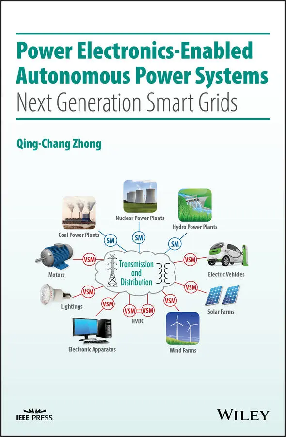
Qing-Chang Zhong - Power Electronics-Enabled Autonomous Power Systems
Здесь есть возможность читать онлайн «Qing-Chang Zhong - Power Electronics-Enabled Autonomous Power Systems» — ознакомительный отрывок электронной книги совершенно бесплатно, а после прочтения отрывка купить полную версию. В некоторых случаях можно слушать аудио, скачать через торрент в формате fb2 и присутствует краткое содержание. Жанр: unrecognised, на английском языке. Описание произведения, (предисловие) а так же отзывы посетителей доступны на портале библиотеки ЛибКат.
- Название:Power Electronics-Enabled Autonomous Power Systems
- Автор:
- Жанр:
- Год:неизвестен
- ISBN:нет данных
- Рейтинг книги:3 / 5. Голосов: 1
-
Избранное:Добавить в избранное
- Отзывы:
-
Ваша оценка:
Power Electronics-Enabled Autonomous Power Systems: краткое содержание, описание и аннотация
Предлагаем к чтению аннотацию, описание, краткое содержание или предисловие (зависит от того, что написал сам автор книги «Power Electronics-Enabled Autonomous Power Systems»). Если вы не нашли необходимую информацию о книге — напишите в комментариях, мы постараемся отыскать её.
Power Electronics-Enabled Autonomous Power Systems — читать онлайн ознакомительный отрывок
Ниже представлен текст книги, разбитый по страницам. Система сохранения места последней прочитанной страницы, позволяет с удобством читать онлайн бесплатно книгу «Power Electronics-Enabled Autonomous Power Systems», без необходимости каждый раз заново искать на чём Вы остановились. Поставьте закладку, и сможете в любой момент перейти на страницу, на которой закончили чтение.
Интервал:
Закладка:
Figure 17.2The closed‐loop system consisting of the power flow model of an inverter and a droop controller.
Figure 17.3Interpretation of transformation matrices T Land T C.
Figure 17.4Interpretation of the universal transformation matrix T .
Figure 17.5Universal droop controller.
Figure 17.6Real‐time simulation results of three inverters with different types of output impedance operated in parallel.
Figure 17.7Experimental set‐up consisting of an L‐inverter, an R‐inverter, and a C‐inverter.
Figure 17.8Experimental results with the universal droop controller.
Figure 18.1The self‐synchronized universal droop controller.
Figure 18.2Experimental results of self‐synchronization with the R‐inverter.
Figure 18.3Experimental results when connecting the R‐inverter to the grid.
Figure 18.4Experimental results with the R‐inverter: performance during the whole experimental process.
Figure 18.5Experimental results with the R‐inverter: regulation of system frequency and voltage in the droop mode.
Figure 18.6Experimental results with the R‐inverter: change in the DC‐bus voltage V DC.
Figure 18.7Experimental results of self‐synchronization with the L‐inverter.
Figure 18.8Experimental results with the L‐inverter: connection to the grid.
Figure 18.9Experimental results with the L‐inverter: performance during the whole experimental process.
Figure 18.10Experimental results with the L‐inverter: regulation of system frequency and voltage in the droop mode.
Figure 18.11Experimental results with the L‐inverter: change in the DC‐bus voltage V DC.
Figure 18.12Experimental results of self‐synchronization with the L‐inverter with the robust droop controller.
Figure 18.13Experimental results from the L‐inverter with the robust droop controller: connection to the grid.
Figure 18.14Experimental results from the L‐inverter with the robust droop controller: performance during the whole experimental process.
Figure 18.15Experimental results from the L‐inverter with the robust droop controller: regulation of system frequency and voltage in the droop mode.
Figure 18.16Experimental results with the L‐inverter under robust droop control: change in the DC‐bus voltage V DC.
Figure 18.17A microgrid including three inverters connected to a weak grid.
Figure 18.18Real‐time simulation results from the microgrid.
Figure 19.1A general three‐port converter with an AC port, a DC port, and a storage port.
Figure 19.2DC‐bus voltage controller to generate the real power reference.
Figure 19.3The universal droop controller when the positive direction of the current is taken as flowing into the converter.
Figure 19.4Finite state machine of the droop‐controlled rectifier.
Figure 19.5Illustration of the operation of the droop‐controlled rectifier.
Figure 19.6The θ‐converter.
Figure 19.7Control structure for the droop‐controlled rectifier.
Figure 19.8Experimental results in the GS mode.
Figure 19.9Experimental results in the NS‐H mode.
Figure 19.10Experimental results in the NS‐L mode.
Figure 19.11Transient response when the system starts up.
Figure 19.12Transient response when a load is connected to the system.
Figure 19.13Experimental results showing the capacity potential of the rectifier: real power P , grid voltage V g, DC‐bus voltage v DC, and Δϕ.
Figure 19.14Controller for the conversion leg.
Figure 19.15Comparative experimental results with a conventional controller.
Figure 20.1A grid‐connected single‐phase inverter with an LCL filter.
Figure 20.2The equivalent circuit diagram of the controller.
Figure 20.3The overall control system.
Figure 20.4Controller states.
Figure 20.5Implementation diagram of the current‐limiting universal droop controller.
Figure 20.6Operation with a normal grid.
Figure 20.7Transient response of the controller states with a normal grid.
Figure 20.8Operation under a grid voltage sag 110 V → 90 V → 110 V for 9 s.
Figure 20.9Controller states under the grid voltage sag 110 V → 90 V → 110 V for 9 s.
Figure 20.10Operation under a grid voltage sag 110 V → 55 V → 110 V for 9 s.
Figure 20.11Controller states under the grid voltage sag 110 V → 55 V → 110 V for 9 s.
Figure 21.1Two systems with disturbances interconnected through Σ I.
Figure 21.2Two systems with disturbances and external ports interconnected through Σ I.
Figure 21.3Three‐phase grid‐connected converter with a local load.
Figure 21.4The controller for a cybersync machine with e to be supplied as u .
Figure 21.5The mathematical structure of the system constructed to facilitate the passivity analysis, where the plant pair Σ Pconsists of the original plant and its ghost in grey and the input to the ghost plant is the ghost of the input to the plant.
Figure 21.6Blocks Σ ωand Σ φimplemented with the IC.
Figure 21.7A cybersync machine equipped with regulation and self‐synchronization.
Figure 21.8Simulation results from a cybersync machine, where the detailed transients indicated by the arrows last for five cycles with the magnitude reduced by 50%.
Figure 21.9Experimental results from a cybersync machine.
Figure 22.1A photo of the SYNDEM smart grid research and educational kit.
Figure 22.2SYNDEM smart grid research and educational kit: main power circuit.
Figure 22.3Implementation of DC–DC converters.
Figure 22.4Implementation of uncontrolled rectifiers.
Figure 22.5Implementation of PWM‐controlled rectifiers.
Figure 22.6Implementation of the θ‐converter.
Figure 22.7Implementation of inverters.
Figure 22.8Implementation of a DC–DC–AC converter.
Figure 22.9Implementation of a single‐phase back‐to‐back converter.
Figure 22.10Implementation of a three‐phase back‐to‐back converter.
Figure 22.11Illustrative structure of the single‐node system.
Figure 22.12Circuit of the single‐node system.
Figure 22.13Experimental results from the single‐node system equipped with a SYNDEM smart grid research and educational kit.
Figure 22.14Texas Tech SYNDEM microgrid built up with eight SYNDEM smart grid research and educational kits
Figure 23.1Illinois Tech SYNDEM smart grid testbed.
Figure 23.2Topology of a θ‐converter.
Читать дальшеИнтервал:
Закладка:
Похожие книги на «Power Electronics-Enabled Autonomous Power Systems»
Представляем Вашему вниманию похожие книги на «Power Electronics-Enabled Autonomous Power Systems» списком для выбора. Мы отобрали схожую по названию и смыслу литературу в надежде предоставить читателям больше вариантов отыскать новые, интересные, ещё непрочитанные произведения.


Обсуждение, отзывы о книге «Power Electronics-Enabled Autonomous Power Systems» и просто собственные мнения читателей. Оставьте ваши комментарии, напишите, что Вы думаете о произведении, его смысле или главных героях. Укажите что конкретно понравилось, а что нет, и почему Вы так считаете.