Javid A. Parray - Nano-Technological Intervention in Agricultural Productivity
Здесь есть возможность читать онлайн «Javid A. Parray - Nano-Technological Intervention in Agricultural Productivity» — ознакомительный отрывок электронной книги совершенно бесплатно, а после прочтения отрывка купить полную версию. В некоторых случаях можно слушать аудио, скачать через торрент в формате fb2 и присутствует краткое содержание. Жанр: unrecognised, на английском языке. Описание произведения, (предисловие) а так же отзывы посетителей доступны на портале библиотеки ЛибКат.
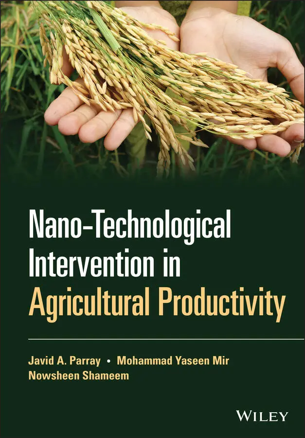
- Название:Nano-Technological Intervention in Agricultural Productivity
- Автор:
- Жанр:
- Год:неизвестен
- ISBN:нет данных
- Рейтинг книги:3 / 5. Голосов: 1
-
Избранное:Добавить в избранное
- Отзывы:
-
Ваша оценка:
Nano-Technological Intervention in Agricultural Productivity: краткое содержание, описание и аннотация
Предлагаем к чтению аннотацию, описание, краткое содержание или предисловие (зависит от того, что написал сам автор книги «Nano-Technological Intervention in Agricultural Productivity»). Если вы не нашли необходимую информацию о книге — напишите в комментариях, мы постараемся отыскать её.
Explores biotechnological advances in the development of sophisticated green technologies for waste minimization and waste control Emphasizes the use of microbes for degradation and removal of various xenobiotic substances Discusses bioremediation approaches in relation to the impact of increased urbanization and industrialization on the environment Covers a variety of applications of nanotechnology in agriculture, including nano-fertilizers, nano-biosensors, nano-pesticides, and nanoparticle protection in plants
is a valuable resource for students in plant biotechnology and agricultural science and engineering, as well as an important reference for researchers in plant biotechnology and agricultural sciences, particularly those with interest in the use of nanomaterials for pollution remediation and sustainable development.
Nano-Technological Intervention in Agricultural Productivity — читать онлайн ознакомительный отрывок
Ниже представлен текст книги, разбитый по страницам. Система сохранения места последней прочитанной страницы, позволяет с удобством читать онлайн бесплатно книгу «Nano-Technological Intervention in Agricultural Productivity», без необходимости каждый раз заново искать на чём Вы остановились. Поставьте закладку, и сможете в любой момент перейти на страницу, на которой закончили чтение.
Интервал:
Закладка:
1.4.2.2 Energy‐Dispersive X‐ray (EDX)
To understand the elementary composition with a rough idea of per cent weight, a usually fixed field emission scanning electron microscopy (FE‐SEM) or TEM system is commonly used. The electron beam centred on a single NP through SEM or TEM through the software functions to obtain the insight knowledge under observation from the NP. NP consists of constituent elements and, by irradiating electron beams, each of these releases X‐ray energy characteristics. The real X‐ray intensity is directly proportional to the explicit part of the particle's concentration. Researchers in preparatory materials commonly use this technique to help SEM and other processes to validate their components [48]. The elemental composition of ultra–sonochemically synthesized BiVO 4NPs in pseudo‐flower form [49] was calculated using the EDX technique. Similarly, a similar approach was used to perform the indispensable confirmation and graphene impregnation of Ln 2O 3/graphene heterostructure NPs, which showed C, Ln, and O as contributing elements synthesized by the traditional hydrothermal method [50].
1.4.2.3 XPS
It is a surface‐sensitive tool and can be used to consider the overall composition and the compositional variance with in‐depth profiling studies. XPS is based on the basic principles of spectroscopy. The typical XPS spectrum consists of the number of electrons on the Y ‐axis plot versus the X ‐axis electrons' binding energy (eV). Each element has its fingerprint value for energy binding and thus gives a particular set of XPS peaks. Corresponding peaks, such as 1s, 2s, 2p, and 3s, come from the electronic configuration [51]. To research the dispersion of Boron NPs (10 nm size) during functionalization with polyethylene glycol (PEG), a depth profile analysis was given with Ar +ions at 1.4 keV and 20 nm. It has been shown that the concentration of NPs increases from 2% to 5% with depth. This offered strong evidence that within the bulk of functionalized PEG, boron NPs are effectively dissolved [52]. In a related analysis, core–shell Au/Ag showed similar behaviour through XPS scope profiling [53].
1.4.2.4 FT‐IR and Raman Spectroscopies
The vibration characterization of NPs is typically studied by FT‐IR and Raman spectroscopies. These techniques are the most evolved and feasible compared to other simple analytical methods. The critical range for NPs is the fingerprint region, which provides the details for the material signature. In one sample, Pt‐NP (1.7 nm) functionalization and its interaction with the alumina substrate were analysed using FT‐IR and XPS techniques. FT‐IR confirms the functionality as it showed signature vibrational peaks of carboxylated C–O 2033 cm −1, in addition to a broader O–H peak of 3280 cm −1, respectively [54, 55]. Because of its signal‐enhancing capability via SPR phenomenon, recently improved surface‐enhanced Raman spectroscopy (SERS) is emerging as a vibrational conforming tool [56, 57].
1.4.3 Particle Size and Surface Area Characterization
Various techniques can calculate the size and surface area of the NPs. These include dispersing SEM, TEM, XRD, AFM, and dynamic light scattering (DLS). It is possible to increase the particle size of SEM, TEM, XRD, and AFM, but the zeta theoretical analyser/DLS should be used to find the NP size at a weak stage. In one study, DLS was used to analyse silica NP size differences while consuming serum proteins. With the acquisition of the protein layer, the findings showed that the size increased. However, in the case of aggregation and hydrophilicity, DLS might prove incapable of accurate measurement, so in that case, we should focus on the high‐resolution technique of differential centrifugal sedimentation [58–60].
1.4.4 Optical Characterizations
Optical characteristics are of great concern in photocatalytic applications, and photochemists have therefore gathered a good understanding of this approach to reveal their photochemical processes [61, 62]. These are based on the common law of Beer–Lambert and the basic principles of light [63]. These methods include information about the absorption, reflectance, luminescence, and phosphorescence of nanomaterials. Metallic and semiconductor NPs have various colours and are thus ideally suited for photo‐related applications. To understand each application's primary mechanism, it is often essential to see the importance of absorption and reflectance of these materials. UV–vis and photoluminescence are the most common optical devices used to study the optical properties of NP materials (PL, Null Ellipsometer). The Diffuse reflectance spectroscopy (DRS) UV/vis is a fully designed optical absorption, transmission, and reflection measurement unit. The first two are extra, while DRS is mostly a unique technique for the samples sold. It is imperative to use the method for measuring NP band gaps as well as other NPs. MMT, LaFeO 3, and LaFeO 3/MMT nanocomposite synthesis and differences in their absorption of electromagnetic radiation by UV–vis DRS to identify their optical characteristics were studied [64]. In the case of nanocomposites, a significant red shift was observed compared to pristine MMT and LaFeO 3NPs. Instead of a broad absorption band from 400 to 620 nm, LaFeO 3and LaFeO 3/MMT revealed a reduction in their band gap. These NPs are significant for photocatalysis by solar light [64]. To investigate the optical properties of photoactive NPs and other nanomaterials and UV, PL considers useful technologies. This technique gives further information on the absorption or emission potential of the materials and their effects on the picture's overall excitement period. It thus provides valuable details about the charging hybridization and half‐life of the exciting material on their conducting bands for all photo‐ and image applications.
1.5 Physicochemical Properties of NPs
Different physicochemical features such as the large surface are discussed; as previously mentioned, mechanically robust, optically active, and chemically reactive NPs are unique and ideal for multiple uses. Some of its essential properties are discussed in the following.
1.5.1 Mechanical and Optical Properties
There is greater interdependence between the optical and electronic properties of NPs. The noble metal NPs, for example, display full UV–visible extinction bands not available on the bulk metal spectrum and have visual properties that are dependent on size. When the conduction electrons' mutual excitation is aroused, this band of enthusiasm results in a continuous photon occurrence, known as the LSPR. LSPR excitation results in wavelength selection absorption with a large Ray light scattering coefficient of molar excitation resonance with an efficiency equal to that of 10 fluorophores and enhanced local electromagnetic fields near the surface of NPs, which strengthened spectroscopy. It is well known that the absorption spectrum of the LSPR spectrum relies on the size, shape, and interparticle spacing of the NPs, as well as its dielectric and local characteristics, such as substrates, solvents, and adsorbents [65]. The rusty colours seen in the door/windows of blemished glass are gold colloidal NPs responsibility, while Ag NPs are usually yellow. The free electrons on the surface are easily transportable via the nanomaterial in these NPs (d electrons in Ag and gold). For Ag and gold, the mean open path is 50 nm, more than the size of these materials in NPs. Thus, no scattering is required from the bulk after weak interaction. Instead, in these NPs, they set up standing resonance conditions responsible for LSPR [66, 67].
1.5.2 Magnetic Properties
Интервал:
Закладка:
Похожие книги на «Nano-Technological Intervention in Agricultural Productivity»
Представляем Вашему вниманию похожие книги на «Nano-Technological Intervention in Agricultural Productivity» списком для выбора. Мы отобрали схожую по названию и смыслу литературу в надежде предоставить читателям больше вариантов отыскать новые, интересные, ещё непрочитанные произведения.


![Chade-Meng Tan - Search Inside Yourself - Increase Productivity, Creativity and Happiness [ePub edition]](/books/703803/chade-thumb.webp)

Обсуждение, отзывы о книге «Nano-Technological Intervention in Agricultural Productivity» и просто собственные мнения читателей. Оставьте ваши комментарии, напишите, что Вы думаете о произведении, его смысле или главных героях. Укажите что конкретно понравилось, а что нет, и почему Вы так считаете.