Rajender Boddula - Fundamentals of Solar Cell Design
Здесь есть возможность читать онлайн «Rajender Boddula - Fundamentals of Solar Cell Design» — ознакомительный отрывок электронной книги совершенно бесплатно, а после прочтения отрывка купить полную версию. В некоторых случаях можно слушать аудио, скачать через торрент в формате fb2 и присутствует краткое содержание. Жанр: unrecognised, на английском языке. Описание произведения, (предисловие) а так же отзывы посетителей доступны на портале библиотеки ЛибКат.
- Название:Fundamentals of Solar Cell Design
- Автор:
- Жанр:
- Год:неизвестен
- ISBN:нет данных
- Рейтинг книги:3 / 5. Голосов: 1
-
Избранное:Добавить в избранное
- Отзывы:
-
Ваша оценка:
Fundamentals of Solar Cell Design: краткое содержание, описание и аннотация
Предлагаем к чтению аннотацию, описание, краткое содержание или предисловие (зависит от того, что написал сам автор книги «Fundamentals of Solar Cell Design»). Если вы не нашли необходимую информацию о книге — напишите в комментариях, мы постараемся отыскать её.
Solar cell-based energy harvesting has attracted worldwide attention for their notable features, such as cheap renewable technology, scalable, lightweight, flexibility, versatility, no greenhouse gas emission, environment, and economy friendly and operational costs are quite low compared to other forms of power generation. Thus, solar cell technology is at the forefront of renewable energy technologies which are used in telecommunications, power plants, small devices to satellites. Aiming at large-scale implementation can be manipulated by various types used in solar cell design and exploration of new materials towards improving performance and reducing cost. Therefore, in-depth knowledge about solar cell design is fundamental for those who wish to apply this knowledge and understanding in industries and academics.
This book provides a comprehensive overview on solar cells and explores the history to evolution and present scenarios of solar cell design, classification, properties, various semiconductor materials, thin films, wafer-scale, transparent solar cells, and so on. It also includes solar cells’ characterization analytical tools, theoretical modeling, practices to enhance conversion efficiencies, applications and patents.
Fundamentals of Solar Cell Design — читать онлайн ознакомительный отрывок
Ниже представлен текст книги, разбитый по страницам. Система сохранения места последней прочитанной страницы, позволяет с удобством читать онлайн бесплатно книгу «Fundamentals of Solar Cell Design», без необходимости каждый раз заново искать на чём Вы остановились. Поставьте закладку, и сможете в любой момент перейти на страницу, на которой закончили чтение.
Интервал:
Закладка:
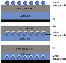
Figure 2.4 Approaches to integrate plasmonic nanoparticle in solar cell.
Plasmonic nanostructures can be used mainly in three manners. First, they can be positioned at the top surface as subwavelength scattering element in solar cell as shown in Figure 2.4a. The metallic nanoparticles dielectric particles are used to get scattering. Metallic nanoparticles are preferred because they can scatter more light than their geometry area. Second, a plasmonic nanostructure can be embedded at the interface or inside the absorber as shown in Figure 2.4b. The plasmonic resonance scatters the light inside the absorber layer and increases absorption at the interface. This design is more preferred in DSSC and single junction PV device. Third, the metallic nanostructure can be positioned as array of nanoparticle or very thin film at the back surface in solar cell as shown in Figure 2.4c. The light travels in a longer path and enhances the absorption. The plasmonic thin film does the task of light trapping and collection of charge carriers [38–40].
2.3 Important Optical Properties
The plasmonic nanostructures are mainly used for increasing light absorption through scattering in plasmonic solar cells. The plasmonic nanostructures are affecting to optical properties such as light trapping, absorption, scattering, resonance wavelength range, and energy levels.
2.3.1 Trapping of Light
The metal nanoparticles are normally placed at a particular distance for trapping enough sunlight between nanoparticle and substrate in solar cell. The illuminated light intensity decreases with distance from the substrate in the case of embedded plasmonic nanoparticle. The top deposited plasmonic nanoparticle design is advantageous for illuminated light into the substrate. The more light escapes from device if there is no distance between the substrate and particle. The absorption is enhanced by folding light in absorber using plasmonic nanoparticles. The folding of light is mainly depending on the structural properties of metallic nanoparticles. The absorption is large in small nanoparticles because of increased near-field. However, very smaller metal nanoparticles go through ohmic loss. Hence, the surface plasmons can be utilized to improve the electric and optical behavior of solar cells. SPRs have ability to collect about 95% incident light where as conventional solar cell can collect about 30% of sunlight [41].
2.3.2 Scattering and Absorption of Sunlight
The absorption and scattering of incident sunlight are main affecting parameters on the efficiency of solar cells. The utilization of plasmonic nanostructures at the top surface of the PV device improves the overall absorption through the scattering of light. For example, silicon does not absorb much light and hence more lights need to be scattered to increase the absorption. The deposited silver metal nanoparticles at the surface increases the absorption and scattering due to surface plasmons is about 10 times more than the nanoparticle. A broader plasmon resonance can be achieved in metal nanoparticles with a large scattering [42].
2.3.3 Multiple Energy Levels
The multiple energy levels are possible by designing the stacks of solar cells on top of each cell with a different energy band gap to increase the absorption of light. The stacked structure of PV cell utilizes maximum sunlight and produces maximum energy conversion efficiency. The each cell should have same lattice parameters to decrease the energy losses [43]. The energy band gap values are summarized for various materials with their maximum absorption wavelength in Table 2.2. The band gap energy vs. λ maxcurve for different photoactive materials is shown in Figure 2.5.
Table 2.2 Energy band gap of various absorber and metal nanoparticles.
| Material | Energy band gap (eV) at 300K | λmax (λ = hc/E = 1242/E) nm |
| Ge | 0.66 | 1,881 |
| Si | 1.11 | 1,118 |
| InP | 1.27 | 977 |
| CIGS | 1.42 | 874 |
| GaAs | 1.43 | 868 |
| CdTe | 1.44 | 862 |
| CZTS | 1.5 | 828 |
| CuO | 1.7 | 730 |
| CdSe | 1.74 | 714 |
| BiFeO 3 | 2.09 | 594 |
| Fe 2O 3 | 2.1 | 591 |
| GaP | 2.25 | 552 |
| CdS | 2.25 | 552 |
| PbO | 2.9 | 428 |
| TiO 2 | 3.2 | 388 |
| SrTiO 3 | 3.2 | 388 |
| ZnO | 3.4 | 365 |
| SnO 2 | 3.5 | 355 |
| ZnS | 3.6 | 345 |
| SiO 2 | 8.9 | 140 |
2.4 Advancements in Plasmonic Solar Cells
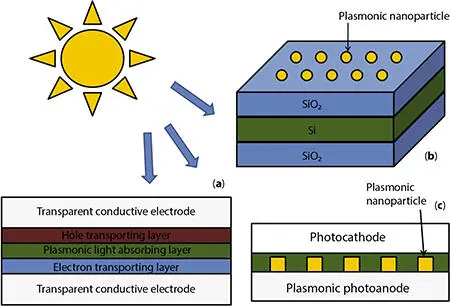
Nanotechnology has huge impact on producing efficient energy conversion devices due to its ability to develop novel materials. There are many experimental reports that confirm the enhancement in light absorption and efficiency because of light scattering from metal nanoparticles in plasmonic solar cells. The plasmonic nanostructures utilize the incident photons with multiple energy values and decrease the loss of photon energies. Researchers are finding the best way to use maximum incident photons for more absorption and high efficiency. The plasmonic solar cells are classified mainly into two categories as direct plasmonic and plasmonicenhanced solar PV cells [44, 45]. The schematic representation of various plasmonic solar cells is shown in Figures 2.6a(direct plasmonic solar cell) and 2.6band 2.6c(plasmonic-enhanced solar cells). The efficiency for various plasmonic solar cell technologies is given in Figure 2.7. The various plasmonic solar cells and its efficiencies are summarized in Table 2.3.
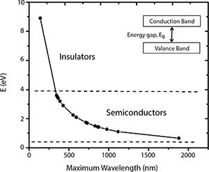
Figure 2.5 Bandgap energy vs. λ maxcurve for various material used in solar cells. The values of this curve that are mentioned correspond to Table 2.2.
2.4.1 Direct Plasmonic Solar Cells
The direct plasmonic solar cells utilize plasmonic nanoparticles as active light absorbers. The hot charge carriers in plasmonic nanoparticles can be produced by excitation of SPR. The hot electrons can be introduced into semiconductor for converting sunlight into electric energy and hot holes can also be injected into a p-type semiconductor. The separation of charge carriers makes possible to use plasmonic nanostructures directly as photo absorbers. The metallic nanoparticles such as Au and Ag offers plasmonic band in visible range that can act as light harvesting antenna. Yocefu Hattori and Jacinto Sa have demonstrated direct plasmonic solar cell using gold surface plasmons [46]. Peafowl solar power company, a spinout company from Uppsala University, Sweden, has started to develop direct plasmonic transparent solar cells for commercial applications. The device configuration of this plasmonic solar cell is similar to traditional thin film PV cell. These plasmonic solar cells were manufactured inexpensively through a printing process at room temperature which can convert the light into electricity under very low light [47–49].
Интервал:
Закладка:
Похожие книги на «Fundamentals of Solar Cell Design»
Представляем Вашему вниманию похожие книги на «Fundamentals of Solar Cell Design» списком для выбора. Мы отобрали схожую по названию и смыслу литературу в надежде предоставить читателям больше вариантов отыскать новые, интересные, ещё непрочитанные произведения.


Обсуждение, отзывы о книге «Fundamentals of Solar Cell Design» и просто собственные мнения читателей. Оставьте ваши комментарии, напишите, что Вы думаете о произведении, его смысле или главных героях. Укажите что конкретно понравилось, а что нет, и почему Вы так считаете.